JAJSO03D November 2011 – April 2022 SN65HVDA100-Q1
PRODUCTION DATA
- 1 特長
- 2 アプリケーション
- 3 概要
- 4 概要 (続き)
- 5 Revision History
- 6 Pin Configuration and Functions
- 7 Specifications
- 8 Parameter Measurement Information
-
9 Detailed Description
- 9.1 Overview
- 9.2 Functional Block Diagram
- 9.3
Feature Description
- 9.3.1 LIN (Local Interconnect Network) Bus
- 9.3.2 TXD (Transmit Input / Output)
- 9.3.3 RXD (Receive Output)
- 9.3.4 VSUP (Supply Voltage)
- 9.3.5 GND (Ground)
- 9.3.6 EN (Enable Input)
- 9.3.7 NWake (High Voltage Wake Up Input)
- 9.3.8 INH (Inhibit Output)
- 9.3.9 TXD Dominant State Timeout
- 9.3.10 Thermal Shutdown
- 9.3.11 Bus Stuck Dominant System Fault: False Wake-Up Lockout
- 9.3.12 Undervoltage on VSUP
- 9.3.13 Unpowered Device Does Not Affect the LIN Bus
- 9.4 Device Functional Modes
- 10Application and Implementation
- 11Power Supply Recommendations
- 12Layout
- 13Device and Documentation Support
- 14Mechanical, Packaging, and Orderable Information
10.2 Typical Application
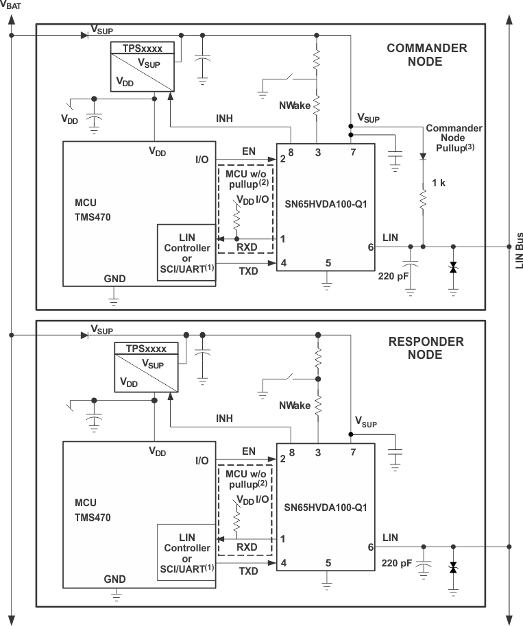
The device comes with an integrated 30-kΩ pullup resistor and series diode for responder applications, and for commander applications an external 1-kΩ pullup with series blocking diode can be used. Figure 10-1 shows the device being used in both types of applications.

A. RXD on MCU or LIN
responder has internal pullup, no external pullup resistor is needed.
B. RXD on MCU or LIN
responder without internal pullup, requires external pullup resistor.
C. Commander node
applications require an external 1-kΩ pullup resistor and serial diode.
Figure 10-1 SN65HVDA100-Q1 Application Diagram