JAJSO47C July   2009  – June 2022 SN65HVDA195-Q1

PRODUCTION DATA  

  1. 特長
  2. アプリケーション
  3. 概要
  4. Revision History
  5. 概要 (続き)
  6. Pin Configuration and Functions
  7. Specifications
    1. 7.1 Absolute Maximum Ratings
    2. 7.2 ESD Ratings
    3. 7.3 Recommended Operating Conditions
    4. 7.4 Thermal Information
    5. 7.5 Electrical Characteristics
    6. 7.6 Typical Characteristics
  8. Parameter Measurement Information
  9. Detailed Description
    1. 9.1 Overview
    2. 9.2 Functional Block Diagram
    3. 9.3 Feature Description
      1. 9.3.1 Local Interconnect Network (LIN) Bus
        1. 9.3.1.1 Transmitter Characteristics
        2. 9.3.1.2 Receiver Characteristics
      2. 9.3.2 Transmit Input (TXD)
      3. 9.3.3 Receive Output (RXD)
        1. 9.3.3.1 RXD Wake-Up Request
      4. 9.3.4 Supply Voltage (VSUP)
      5. 9.3.5 Ground (GND)
      6. 9.3.6 Enable Input (EN)
      7. 9.3.7 NWake Input (NWake)
      8. 9.3.8 Inhibit Output (INH)
    4. 9.4 Device Functional Modes
      1. 9.4.1 Operating Modes
      2. 9.4.2 Normal Mode
      3. 9.4.3 Sleep Mode
      4. 9.4.4 Wake-Up Events
      5. 9.4.5 Standby Mode
  10. 10Application and Implementation
    1. 10.1 Application Information
      1. 10.1.1 Typical Application
        1. 10.1.1.1 Design Requirements
        2. 10.1.1.2 Detailed Design Procedure
        3. 10.1.1.3 Application Curves
      2.      Power Supply Recommendations
      3. 10.1.2 Layout
        1. 10.1.2.1 Layout Guidelines
        2. 10.1.2.2 Layout Example
  11. 11Device and Documentation Support
    1. 11.1 Receiving Notification of Documentation Updates
    2. 11.2 サポート・リソース
    3. 11.3 Trademarks
    4. 11.4 Electrostatic Discharge Caution
    5. 11.5 Glossary
  12. 12Mechanical, Packaging, and Orderable Information

パッケージ・オプション

メカニカル・データ(パッケージ|ピン)
サーマルパッド・メカニカル・データ
発注情報

Standby Mode

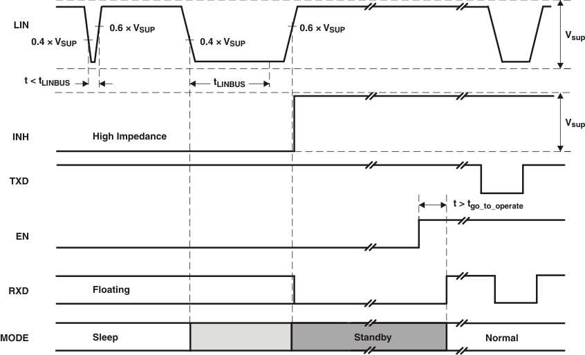
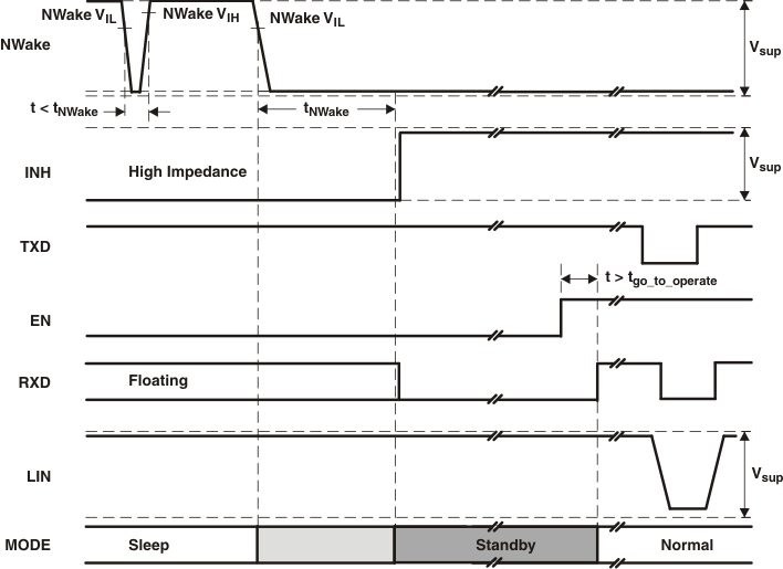
This mode is entered whenever a wake-up event occurs through LIN bus or NWake while the SN65HVDA195 is in sleep mode. The LIN bus responder termination circuit and INH are turned on when standby mode is entered. The application system powers up once INH is turned on, assuming the system is using a voltage regulator connected through INH. Standby mode is signaled through a low level on RXD.

When EN is set high while the SN65HVDA195 is in standby mode the device returns to normal mode and the normal transmission paths from TXD to LIN bus and LIN bus to RXD are enabled.
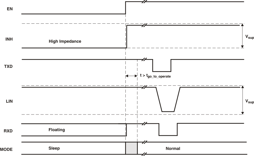
GUID-27D4FDE8-53A5-46A5-A9E2-1FA1F9790F7E-low.gifFigure 9-2 Wakeup Through EN
GUID-8DBAA518-9EC5-4D1F-9B59-DADD6D879F2D-low.gifFigure 9-3 Wakeup Through LIN
GUID-421FFBA1-A274-41BA-B83C-F90123D60B8A-low.gifFigure 9-4 Wakeup Through NWake