JAJSCO6 November 2016 SN65LBC173A-EP
PRODUCTION DATA.
9 Application and Implementation
NOTE
Information in the following applications sections is not part of the TI component specification, and TI does not warrant its accuracy or completeness. TI’s customers are responsible for determining suitability of components for their purposes. Customers should validate and test their design implementation to confirm system functionality.
9.1 Application Information
Extending SPI operation over RS-485 link.
9.2 Typical Application
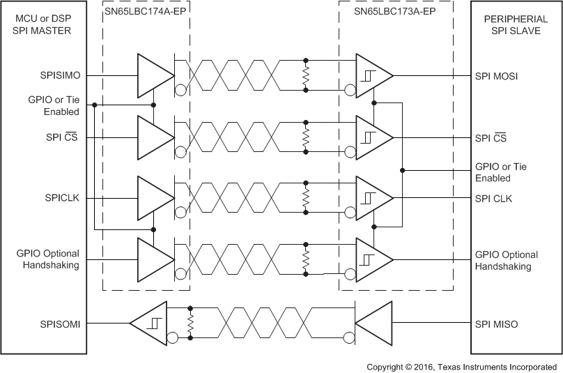
The following block diagram shows an MCU host connected via RS-485 to a SPI slave device. This device can be an ADC, DAC, MCU, or other SPI slave peripheral.
 Figure 12. DSP-to-DSP Link via Serial Peripheral Interface
9.2.1 Design Requirements
This application can be implemented using standard SPI protocol on DSP or MCU devices. The interface is independent of the specific frame or data requirements of the host or slave device. An additional but not required handshake bit is provided that can be used for customer purposes.
9.2.2 Detailed Design Procedure
The interface design requirements are fairly straight forward in this single source/destination scenario. Trace lengths and cable lengths need to be matched to maximize SPI timing. If there is a benefit to put the interface to sleep, GPIOs can be used to control the enable signals of the transmitter and receiver. If GPIOs are not available, or constant uptime needed, both the enables on transmit and receive can be hard tied enabled.
The link shown can operate at up to 50 Mbps, well within the capability of most SPI links.
9.2.3 Application Curves
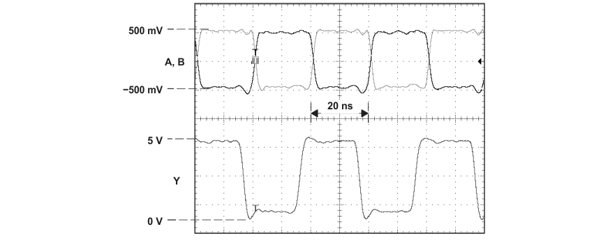
 Figure 13. Receiver Inputs and Outputs, 50-Mbps Signaling Rate