JAJSCO6 November 2016 SN65LBC173A-EP
PRODUCTION DATA.
11 Layout
11.1 Layout Guidelines
For best operational performance of the device, use good PCB layout practices including:
- Noise can propagate into analog circuitry through the power pins of the circuit as a whole, as well as the operational amplifier. Bypass capacitors are used to reduce the coupled noise by providing low impedance power sources local to the analog circuitry.
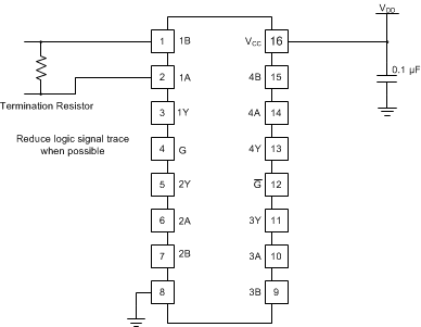
- Connect low-ESR, 0.1-μF ceramic bypass capacitors between each supply pin and ground, placed as close to the device as possible.
- Place termination resistor as close as possible to the input pins (if end point node).
- Keep trace lengths from input pins to buss as short as possible to reduce stub lengths and reflections on any nodes that are not end points of bus.
- To reduce parasitic coupling, run the input traces as far away from the supply or output traces as possible. If it is not possible to keep them separate, it is much better to cross the sensitive trace perpendicular as opposed to in parallel with the noisy trace.
11.2 Layout Example
 Figure 14. Layout with PCB Recommendations