JAJSV24J October 1996 – July 2024 SN65LBC184 , SN75LBC184
PRODUCTION DATA
- 1
- 1 特長
- 2 アプリケーション
- 3 概要
- 4 Pin Configuration and Functions
-
5 Specifications
- 5.1 Absolute Maximum Ratings
- 5.2 ESD Ratings
- 5.3 Recommended Operating Conditions
- 5.4 Thermal Information
- 5.5 Electrical Characteristics: Driver
- 5.6 Electrical Characteristics: Receiver
- 5.7 Driver Switching Characteristics
- 5.8 Receiver Switching Characteristics
- 5.9 Dissipation Ratings
- 5.10 Typical Characteristics
- 6 Parameter Measurement Information
- 7 Detailed Description
- 8 Application and Implementation
- 9 Device and Documentation Support
- 10Revision History
- 11Mechanical, Packaging, and Orderable Information
パッケージ・オプション
メカニカル・データ(パッケージ|ピン)
サーマルパッド・メカニカル・データ
発注情報
8.2.2.1 SN65LBC184 Test Description
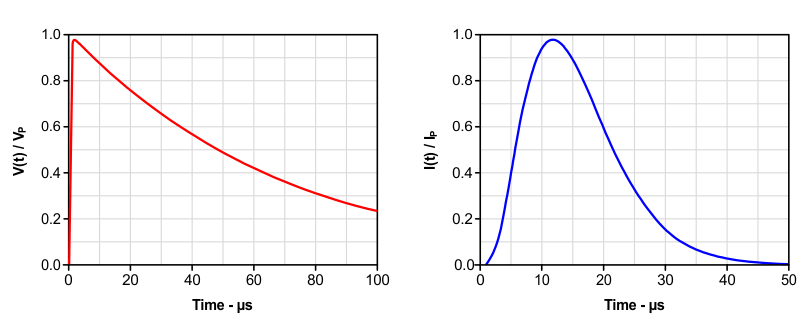
The SN65LBC184 is tested against the IEC 61000-4-5 recommended transient identified as the combination wave. The combination wave provides a 1.2-/50μs open-circuit voltage waveform and a 8-/20μs short-circuit current waveform shown in Figure 8-4. The testing is performed with a combination/hybrid pulse generator with an effective output impedance of 2Ω. The setup for the overvoltage stress is shown in Figure 8-5 with all testing performed with power applied to the SN65LBC184 circuit.
 Figure 8-4 Open-Circuit Voltage and Short-Circuit Current Waveforms
The SN65LBC184 is tested and evaluated for both maximum (single pulse) as well as life test (multiple pulse) capabilities. The SN65LBC184 is evaluated against transients of both positive and negative polarity and all testing is performed with the worst-case transient polarity. Transient pulses are applied to the bus pins (A and B) across ground as shown in Figure 8-5.
 Figure 8-5 Overvoltage Stress Test Circuit