JAJSF11B August   2009  – March 2015 SN65LVDS93A

PRODUCTION DATA.  

  1. 特長
  2. アプリケーション
  3. 概要
    1.     Device Images
      1.      ディスクリートLVDS TXを使用するRGBビデオ・システム
  4. 改訂履歴
  5. 概要(続き)
  6. Pin Configuration and Functions
    1.     Pin Functions - TSSOP
    2.     Pin Functions - BGA MICROSTAR
  7. Specifications
    1. 7.1 Absolute Maximum Ratings
    2. 7.2 ESD Ratings
    3. 7.3 Recommended Operating Conditions
    4. 7.4 Thermal Information
    5. 7.5 Electrical Characteristics
    6. 7.6 Timing Requirements
    7. 7.7 Switching Characteristics
    8. 7.8 Typical Characteristics
  8. Parameter Measurement Information
  9. Detailed Description
    1. 9.1 Overview
    2. 9.2 Functional Block Diagram
    3. 9.3 Feature Description
      1. 9.3.1 TTL Input Data
      2. 9.3.2 LVDS Output Data
    4. 9.4 Device Functional Modes
      1. 9.4.1 Input Clock Edge
      2. 9.4.2 Low Power Mode
  10. 10Application and Implementation
    1. 10.1 Application Information
    2. 10.2 Typical Application
      1. 10.2.1 Design Requirements
      2. 10.2.2 Detailed Design Procedure
        1. 10.2.2.1 Power
        2. 10.2.2.2 Signal Connectivity
        3. 10.2.2.3 PCB Routing
      3. 10.2.3 Application Curve
  11. 11Power Supply Recommendations
  12. 12Layout
    1. 12.1 Layout Guidelines
      1. 12.1.1 Board Stackup
      2. 12.1.2 Power and Ground Planes
      3. 12.1.3 Traces, Vias, and Other PCB Components
    2. 12.2 Layout Example
  13. 13デバイスおよびドキュメントのサポート
    1. 13.1 ドキュメントのサポート
      1. 13.1.1 関連資料
    2. 13.2 ドキュメントの更新通知を受け取る方法
    3. 13.3 コミュニティ・リソース
    4. 13.4 商標
    5. 13.5 静電気放電に関する注意事項
    6. 13.6 Glossary
  14. 14メカニカル、パッケージ、および注文情報

パッケージ・オプション

メカニカル・データ(パッケージ|ピン)
サーマルパッド・メカニカル・データ
発注情報

Typical Characteristics

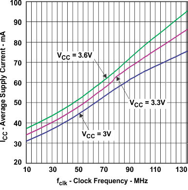
SN65LVDS93A gscale_v_clk_llsem1.gif
Total device current (using grayscale pattern) over pixel clock frequency
Figure 2. Average Grayscale ICC vs Clock Frequency
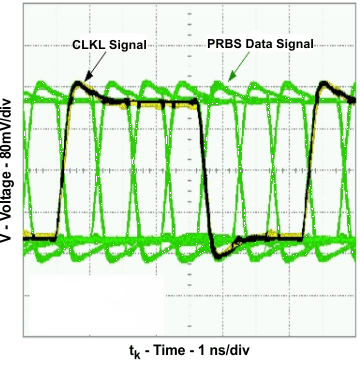
SN65LVDS93A typ_prbs_llsem1.gif
Clock signal = 135 MHz
Figure 4. Typical PRBS Output Signal
Over One Clock Period
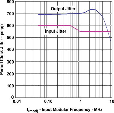
SN65LVDS93A outjit_v_freq_llsem1.gif
CLK frequency during text = 100 MHz
Figure 3. Output Clock Jitter vs Input Clock Jitter