JAJSKL9B September 2020 – November 2022 SN65MLVD203B
PRODUCTION DATA
- 1 特長
- 2 アプリケーション
- 3 概要
- 4 Revision History
- 5 Pin Configuration and Functions
- 6 Specifications
- 7 Parameter Measurement Information
- 8 Detailed Description
-
9 Application and Implementation
- 9.1 Application Information
- 9.2
Typical Application
- 9.2.1 Multipoint Communications
- 9.2.2 Design Requirements
- 9.2.3
Detailed Design Procedure
- 9.2.3.1 Supply Voltage
- 9.2.3.2 Supply Bypass Capacitance
- 9.2.3.3 Driver Input Voltage
- 9.2.3.4 Driver Output Voltage
- 9.2.3.5 Termination Resistors
- 9.2.3.6 Receiver Input Signal
- 9.2.3.7 Receiver Input Threshold (Failsafe)
- 9.2.3.8 Receiver Output Signal
- 9.2.3.9 Interconnecting Media
- 9.2.3.10 PCB Transmission Lines
- 9.2.4 Application Curves
- 9.3 Power Supply Recommendations
- 9.4 Layout
- 10Device and Documentation Support
- 11Mechanical, Packaging, and Orderable Information
パッケージ・オプション
メカニカル・データ(パッケージ|ピン)
- RUM|16
サーマルパッド・メカニカル・データ
- RUM|16
発注情報
9.2.1 Multipoint Communications
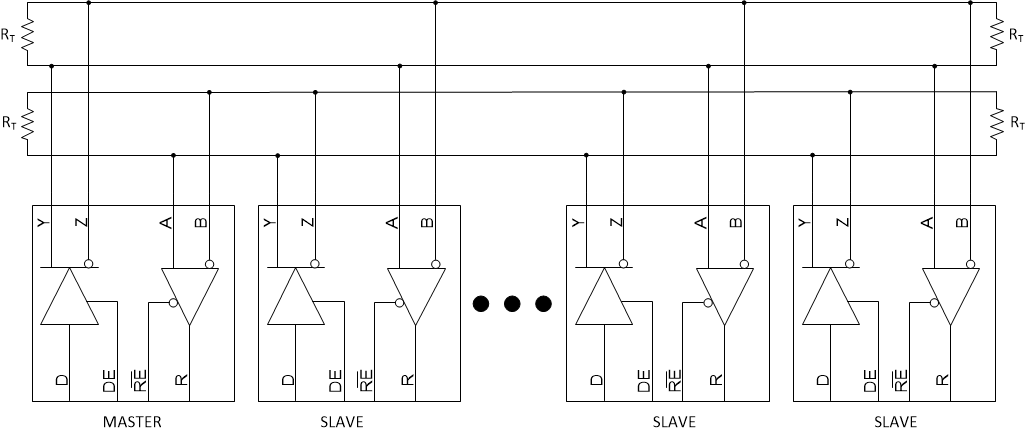
In a multipoint configuration many transmitters and many receivers can be interconnected on a single transmission line. The key difference compared to multi-drop is the presence of two or more drivers. Such a situation creates contention issues that need not be addressed with point-to-point or multidrop systems. Multipoint operation allows for bidirectional, half-duplex communication over a single balanced media pair. To support the location of the various drivers throughout the transmission line, double termination of the transmission line is now necessary.
The major challenge that system designers encounter are the impedance discontinuities that device loading and device connections (stubs) introduce on the common bus. Matching the impedance of the loaded bus and using signal drivers with controlled signal edges are the keys to error-free signal transmissions in multipoint topologies.
 Figure 9-1 Multipoint Configuration