JAJSFV6A August 2018 – January 2019 SN74AXCH8T245
PRODUCTION DATA.
- 1 特長
- 2 アプリケーション
- 3 概要
- 4 改訂履歴
- 5 概要(続き)
- 6 Pin Configuration and Functions
-
7 Specifications
- 7.1 Absolute Maximum Ratings
- 7.2 ESD Ratings
- 7.3 Recommended Operating Conditions
- 7.4 Thermal Information
- 7.5 Electrical Characteristics
- 7.6 Switching Characteristics, VCCA = 0.7 V
- 7.7 Switching Characteristics, VCCA = 0.8 V
- 7.8 Switching Characteristics, VCCA = 0.9 V
- 7.9 Switching Characteristics, VCCA = 1.2 V
- 7.10 Switching Characteristics, VCCA = 1.5 V
- 7.11 Switching Characteristics, VCCA = 1.8 V
- 7.12 Switching Characteristics, VCCA = 2.5 V
- 7.13 Switching Characteristics, VCCA = 3.3 V
- 7.14 Operating Characteristics: TA = 25°C
- 8 Parameter Measurement Information
- 9 Detailed Description
- 10Application and Implementation
- 11Power Supply Recommendations
- 12Layout
- 13デバイスおよびドキュメントのサポート
- 14メカニカル、パッケージ、および注文情報
パッケージ・オプション
メカニカル・データ(パッケージ|ピン)
サーマルパッド・メカニカル・データ
発注情報
8 Parameter Measurement Information
Unless otherwise noted, all input pulses are supplied by generators having the following characteristics:
- f =1 MHz
- Z0 = 50 Ω
- dv / dt ≤ 1 ns/V

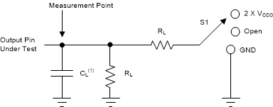
1. CL includes probe and jig capacitance.
Figure 1. Load Circuit 
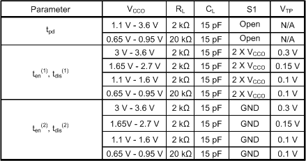
1. Output waveform on the conditions that input is driven to a valid Logic Low.
2. Output waveform on the condition that input is driven to a valid Logic High.
Figure 2. Load Circuit Conditions 
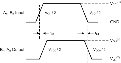
1. VCCI is the supply pin associated with the input port.
2. VOH and VOL are typical output voltage levels with specified RL, CL, and S1.
Figure 3. Propagation Delay 
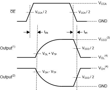
1. Output waveform on the condition that input is driven to a valid Logic Low.
2. Output waveform on the condition that input is driven to a valid Logic High.
3. VCCO is the supply pin associated with the output port.
4. VOH and VOL are typical output voltage levels with specified RL, CL, and S1.
Figure 4. Enable Time And Disable Time