JAJSR18 August 2023 SN74HC165B-EP
PRODUCTION DATA
- 1
- 1 特長
- 2 アプリケーション
- 3 概要
- 4 Revision History
- 5 Pin Configuration and Functions
-
6 Specifications
- 6.1 Absolute Maximum Ratings
- 6.2 ESD Ratings
- 6.3 Recommended Operating Conditions
- 6.4 Thermal Information
- 6.5 Electrical Characteristics
- 6.6 Timing Requirements, VCC = 2 V
- 6.7 Timing Requirements, VCC = 4.5 V
- 6.8 Timing Requirements, VCC = 6 V
- 6.9 Switching Characteristics, VCC = 2 V
- 6.10 Switching Characteristics, VCC = 4.5 V
- 6.11 Switching Characteristics, VCC = 6 V
- 6.12 Operating Characteristics
- 6.13 Typical Characteristics
- 7 Parameter Measurement Information
- 8 Detailed Description
- 9 Application and Implementation
- 10Device and Documentation Support
- 11Mechanical, Packaging, and Orderable Information
7 Parameter Measurement Information
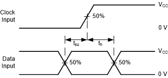
- Phase relationships between waveforms were chosen arbitrarily. All input pulses are supplied by generators having the following characteristics: PRR ≤ 1 MHz, ZO = 50 Ω, tt < 6 ns.
- The outputs are measured one at a time, with one input transition per measurement.

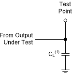
A. CL= 50 pF and includes probe and jig capacitance.
Figure 7-1 Load Circuit Figure 7-3 Voltage Waveforms Setup and Hold Times
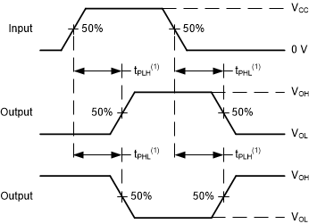
A. The maximum between tPLH and TPHL is used for tpd.
Figure 7-5 Voltage Waveforms Propagation Delays
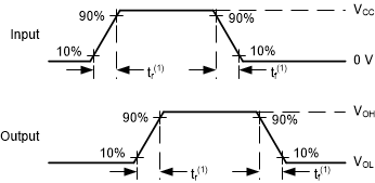
A. The maximum between
tr and tf is used for
tt.
Figure 7-2 Voltage Waveforms Transition Times Figure 7-4 Voltage Waveforms Pulse Width