JAJSI39 October   2019 SN74HCS72-Q1

PRODUCTION DATA.  

  1. 特長
  2. アプリケーション
  3. 概要
    1.     Device Images
      1.      シュミットトリガ入力の利点
  4. 改訂履歴
  5. Pin Configuration and Functions
    1.     Pin Functions
  6. Specifications
    1. 6.1 Absolute Maximum Ratings
    2. 6.2 ESD Ratings
    3. 6.3 Recommended Operating Conditions
    4. 6.4 Thermal Information
    5. 6.5 Electrical Characteristics
    6. 6.6 Switching Characteristics
    7. 6.7 Timing Characteristics
    8. 6.8 Typical Characteristics
  7. Parameter Measurement Information
  8. Detailed Description
    1. 8.1 Overview
    2. 8.2 Functional Block Diagram
    3. 8.3 Feature Description
      1. 8.3.1 Balanced CMOS Push-Pull Outputs
      2. 8.3.2 CMOS Schmitt-Trigger Inputs
      3. 8.3.3 Positive and Negative Clamping Diodes
    4. 8.4 Device Functional Modes
  9. Application and Implementation
    1. 9.1 Application Information
    2. 9.2 Typical Application
      1. 9.2.1 Design Requirements
        1. 9.2.1.1 Output Considerations
        2. 9.2.1.2 Input Considerations
        3. 9.2.1.3 Timing Considerations
      2. 9.2.2 Detailed Design Procedure
      3. 9.2.3 Application Curve
  10. 10Power Supply Recommendations
  11. 11Layout
    1. 11.1 Layout Guidelines
    2. 11.2 Layout Example
  12. 12デバイスおよびドキュメントのサポート
    1. 12.1 ドキュメントのサポート
      1. 12.1.1 関連資料
    2. 12.2 ドキュメントの更新通知を受け取る方法
    3. 12.3 コミュニティ・リソース
    4. 12.4 商標
    5. 12.5 静電気放電に関する注意事項
    6. 12.6 Glossary
  13. 13メカニカル、パッケージ、および注文情報

パッケージ・オプション

メカニカル・データ(パッケージ|ピン)
サーマルパッド・メカニカル・データ
発注情報

Typical Characteristics

TA = 25°C
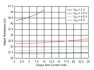
SN74HCS72-Q1 typ_nfet_res.gifFigure 1. Output driver resistance in LOW state.
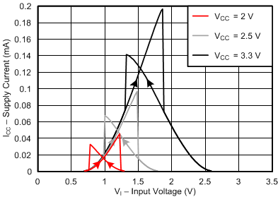
SN74HCS72-Q1 typ-vin-icc-lowv.gifFigure 3. Supply current across input voltage, 2-, 2.5-, and 3.3-V supply
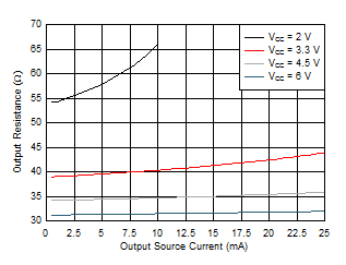
SN74HCS72-Q1 typ_pfet_res.gifFigure 2. Output driver resistance in HIGH state.
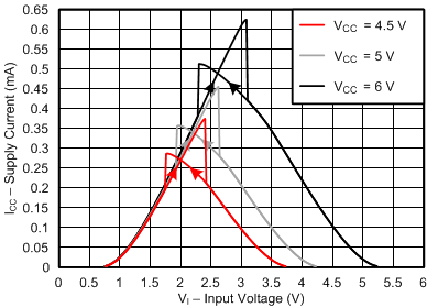
SN74HCS72-Q1 typ-vin-icc-highv.gifFigure 4. Supply current across input voltage, 4.5-, 5-, and 6-V supply