JAJSUQ9M May 1999 – September 2024 SN74LV4053A
PRODUCTION DATA
- 1
- 1 特長
- 2 アプリケーション
- 3 概要
- 4 Pin Configuration and Functions
-
5 Specifications
- 5.1 Absolute Maximum Ratings
- 5.2 ESD Ratings
- 5.3 Thermal Information: SN74LV4053A
- 5.4 Recommended Operating Conditions
- 5.5 Electrical Characteristics
- 5.6 Timing Characteristics VCC = 2.5 V ± 0.2 V
- 5.7 Timing Characteristics VCC = 3.3 V ± 0.3 V
- 5.8 Timing Characteristics VCC = 5 V ± 0.5 V
- 5.9 AC Characteristics
- 6 Parameter Measurement Information
- 7 Detailed Description
- 8 Application and Implementation
- 9 Device and Documentation Support
- 10Revision History
- 11Mechanical, Packaging, and Orderable Information
パッケージ・オプション
デバイスごとのパッケージ図は、PDF版データシートをご参照ください。
メカニカル・データ(パッケージ|ピン)
- PW|16
- DB|16
- DYY|16
- NS|16
- N|16
- RGY|16
- D|16
- DGV|16
サーマルパッド・メカニカル・データ
- RGY|16
発注情報
4 Pin Configuration and Functions
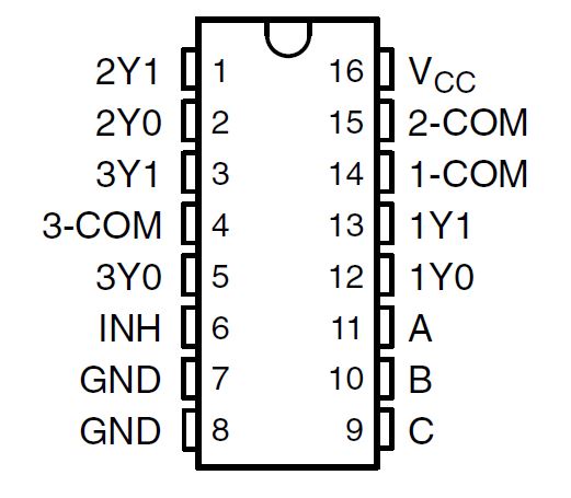
 Figure 4-1 SN74LV4053A D, PW or DYY Packages,
16-Pin SOIC, TSSOP or SOT-23-THIN (Top View)
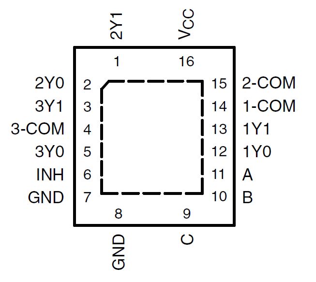
 Figure 4-2 SN74LV4053A RGY, 16-Pin VQFN (Top View)
Table 4-1 Pin Functions
| PIN | TYPE(2) | DESCRIPTION | |
|---|---|---|---|
| NAME | NO. | ||
| 2Y1 | 1 | I(1) | Input to mux 2 |
| 2Y0 | 2 | I(1) | Input to mux 2 |
| 3Y1 | 3 | I(1) | Input to mux 3 |
| 3-COM | 4 | O(1) | Output of mux 3 |
| 3Y0 | 5 | I(1) | Input to mux 3 |
| INH | 6 | I | Enables the outputs of the device. Logic low level with turn the outputs on, high level will turn them off. |
| GND | 7 | - | Ground |
| GND | 8 | - | Ground |
| C | 9 | I | Selector line for outputs (see Section 7.2 for specific information) |
| B | 10 | I | Selector line for outputs (see Section 7.2 for specific information) |
| A | 11 | I | Selector line for outputs (see Section 7.2 for specific information) |
| 1Y0 | 12 | I(1) | Input to mux 1 |
| 1Y1 | 13 | I(1) | Input to mux 1 |
| 1-COM | 14 | O(1) | Output of mux 1 |
| 2-COM | 15 | O(1) | Output of mux 2 |
| VCC | 16 | I | Device power input |
(1) These I/O descriptions represent the device when used as a multiplexer,
when this device is operated as a demultiplexer pins 1Y0, 1Y1, 2Y0, 2Y1, 3Y0, 3Y1 may be
considered outputs (O) and pins 1-COM, 2-COM, and 3-COM may be considered inputs (I).
(2) I = input, O = output