JAJSUQ9M May 1999 – September 2024 SN74LV4053A
PRODUCTION DATA
- 1
- 1 特長
- 2 アプリケーション
- 3 概要
- 4 Pin Configuration and Functions
-
5 Specifications
- 5.1 Absolute Maximum Ratings
- 5.2 ESD Ratings
- 5.3 Thermal Information: SN74LV4053A
- 5.4 Recommended Operating Conditions
- 5.5 Electrical Characteristics
- 5.6 Timing Characteristics VCC = 2.5 V ± 0.2 V
- 5.7 Timing Characteristics VCC = 3.3 V ± 0.3 V
- 5.8 Timing Characteristics VCC = 5 V ± 0.5 V
- 5.9 AC Characteristics
- 6 Parameter Measurement Information
- 7 Detailed Description
- 8 Application and Implementation
- 9 Device and Documentation Support
- 10Revision History
- 11Mechanical, Packaging, and Orderable Information
パッケージ・オプション
デバイスごとのパッケージ図は、PDF版データシートをご参照ください。
メカニカル・データ(パッケージ|ピン)
- PW|16
- DB|16
- DYY|16
- NS|16
- N|16
- RGY|16
- D|16
- DGV|16
サーマルパッド・メカニカル・データ
発注情報
6 Parameter Measurement Information
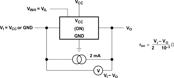 Figure 6-1 On-State Resistance Test Circuit
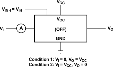 Figure 6-2 Off-State Switch Leakage-Current Test Circuit
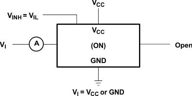 Figure 6-3 On-State Switch Leakage-Current Test Circuit
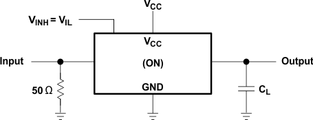 Figure 6-4 Propagation Delay Time, Signal Input to Signal Output
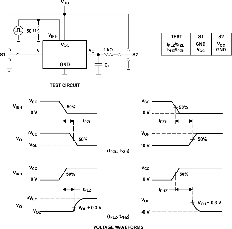 Figure 6-5 Switching Time (tPZL, tPLZ, tPZH,
tPHZ), Control to Signal Output
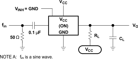 Figure 6-6 Frequency Response (Switch On)
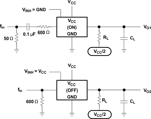 Figure 6-7 Crosstalk Between Any Two Switches
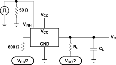 Figure 6-8 Crosstalk Between Control Input and Switch Output
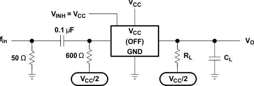 Figure 6-9 Feedthrough Attenuation (Switch Off)
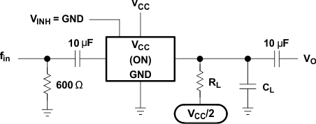 Figure 6-10 Sine-Wave Distortion