JAJSMP5 May 2022 SN74LXC1T14
PRODUCTION DATA
- 1 特長
- 2 アプリケーション
- 3 概要
- 4 Revision History
- 5 Pin Configuration and Functions
- 6 Specifications
- 7 Parameter Measurement Information
-
8 Detailed Description
- 8.1 Overview
- 8.2 Functional Block Diagram
- 8.3
Feature Description
- 8.3.1 CMOS Schmitt-Trigger Inputs with Integrated Pulldowns
- 8.3.2 Balanced High-Drive CMOS Push-Pull Outputs
- 8.3.3 Partial Power Down (Ioff)
- 8.3.4 VCC Isolation and VCC Disconnect (Ioff-float)
- 8.3.5 Over-Voltage Tolerant Inputs
- 8.3.6 Glitch-Free Power Supply Sequencing
- 8.3.7 Negative Clamping Diodes
- 8.3.8 Fully Configurable Dual-Rail Design
- 8.3.9 Supports High-Speed Translation
- 8.4 Device Functional Modes
- 9 Application and Implementation
- 10Power Supply Recommendations
- 11Layout
- 12Device and Documentation Support
- 13Mechanical, Packaging, and Orderable Information
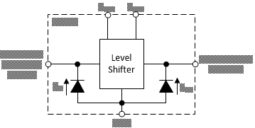
8.3.7 Negative Clamping Diodes
The inputs and outputs to this device have negative clamping diodes as depicted in Figure 8-2.
CAUTION:
Voltages beyond the values specified in the Absolute Maximum Ratings table can cause damage to the device. The input negative-voltage and output voltage ratings may be exceeded if the input and output clamp-current ratings are observed.
 Figure 8-2 Electrical Placement of Clamping Diodes for Each
Input and Output