SLRS021D December 1967 – January 2017 SN55451B , SN55452B , SN55453B , SN55454B , SN75451B , SN75452B , SN75453B , SN75454B
PRODUCTION DATA.
- 1 Features
- 2 Applications
- 3 Description
- 4 Revision History
- 5 Device Comparison Table
- 6 Pin Configuration and Functions
- 7 Specifications
- 8 Parameter Measurement Information
- 9 Detailed Description
- 10Application and Implementation
- 11Power Supply Recommendations
- 12Layout
- 13Device and Documentation Support
- 14Mechanical, Packaging, and Orderable Information
パッケージ・オプション
デバイスごとのパッケージ図は、PDF版データシートをご参照ください。
メカニカル・データ(パッケージ|ピン)
- D|8
- P|8
- PS|8
サーマルパッド・メカニカル・データ
- PS|8
発注情報
9 Detailed Description
9.1 Overview
The SN7545xB and SN5545xB devices provide dual-output drivers with AND, NAND, NOR, or OR logic inputs. If each logic input is set to the appropriate voltage level, then the output driver will turn on, pulling the driver to ground and allowing current to flow.
9.2 Functional Block Diagrams
 Figure 6. SNx5451B Logic Diagram (Positive Logic)
 Figure 7. SNx5452B Logic Diagram (Positive Logic)
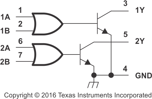
 Figure 8. SNx5453B Logic Diagram (Positive Logic)
 Figure 9. SNx5454B Logic Diagram (Positive Logic)
9.3 Feature Description
The SNx5451B devices allow for high current driving up to 300 mA. This family of devices have AND, NAND, OR, or NOR input logic gates to allow for a wide variety of applications. The SN7545xB devices are rated for a commercial temperature range of 0°C to 70°C, and the SN5545xB devices are rated for a military temperature range of –65°C to 125°C.
9.4 Device Functional Modes
Table 1, Table 2, Table 3, and Table 4 list the functional modes of the SNx545xB.
 Figure 10. SNx5451B Logic Symbol
Table 1. SNx5451B Function Table
| A | B | Y (1) |
|---|---|---|
| L | L | L (on state) |
| L | H | L (on state) |
| H | L | L (on state) |
| H | H | H (off state) |
 Figure 11. SNx5452B Logic Symbol
Table 2. SNx5452B Function Table
| A | B | Y (1) |
|---|---|---|
| L | L | H (off state) |
| L | H | H (off state) |
| H | L | H (off state) |
| H | H | L (on state) |
 Figure 12. SNx5453B Logic Symbol
Table 3. SNx5453B Function Table
| A | B | Y (1) |
|---|---|---|
| L | L | L (on state) |
| L | H | H (off state) |
| H | L | H (off state) |
| H | H | H (off state) |
 Figure 13. SNx5454B Logic Symbol
Table 4. SNx5454B Function Table
| A | B | Y (1) |
|---|---|---|
| L | L | H (off state) |
| L | H | L (on state) |
| H | L | L (on state) |
| H | H | L (on state) |
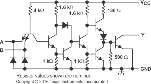
 Figure 14. SNx5451B Schematic (Each Driver)
 Figure 16. SNx5453B Schematic (Each Driver)
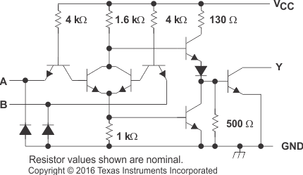
 Figure 15. SNx5452B Schematic (Each Driver)
 Figure 17. SNx5454B Schematic (Each Driver)