JAJSP94G January 1994 – October 2022 SN65LBC179 , SN75LBC179
PRODUCTION DATA
- 1特長
- 2概要
- 3Revision History
- 4Pin Configuration and Functions
-
5Specifications
- 5.1 Absolute Maximum Ratings
- 5.2 Recommended Operating Conditions
- 5.3 Thermal Information
- 5.4 Dissipation Rating Table
- 5.5 Electrical Characteristics - Driver
- 5.6 Switching Characteristics - Driver
- 5.7 Electrical Characteristics - Receiver
- 5.8 Switching Characteristics - Receiver
- 5.9 Typical Characteristics
- 6Parameter Measurement Information
- 7Detailed Description
- 8Device and Documentation Support
- 9Mechanical, Packaging, and Orderable Information
パッケージ・オプション
メカニカル・データ(パッケージ|ピン)
サーマルパッド・メカニカル・データ
発注情報
4 Pin Configuration and Functions
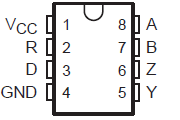
 Figure 4-1 D or P Package (Top View)
Table 4-1 Pin Functions
| PIN | TYPE(1) | DESCRIPTION | |
|---|---|---|---|
| NAME | NO. | ||
| 1 | VCC | P | 5 V Voltage Supply |
| 2 | R | O | RS485 Logic Output |
| 3 | D | I | RS485 Logic Input |
| 4 | GND | G | Ground |
| 5 | Y | O | Non-Inverting RS485 Bus Output |
| 6 | Z | O | Inverted RS485 Bus Output |
| 7 | B | I | Inverted RS485 Bus Input |
| 8 | A | I | Non-Inverting RS485 Bus Input |
(1) I = Input, O = Output, I/O = Input or Output, G = Ground, P = Power.