SLLS362G SEPTEMBER 1999 – January 2016 SN65LVDS387 , SN65LVDS389 , SN65LVDS391 , SN75LVDS387 , SN75LVDS389 , SN75LVDS391
PRODUCTION DATA.
- 1 Features
- 2 Applications
- 3 Description
- 4 Revision History
- 5 Description (Continued)
- 6 Device Options
- 7 Pin Configuration and Functions
- 8 Specifications
- 9 Parameter Measurement Information
- 10Detailed Description
- 11Application and Implementation
- 12Power Supply Recommendations
- 13Layout
- 14Device and Documentation Support
- 15Mechanical, Packaging, and Orderable Information
パッケージ・オプション
デバイスごとのパッケージ図は、PDF版データシートをご参照ください。
メカニカル・データ(パッケージ|ピン)
- DGG|64
サーマルパッド・メカニカル・データ
発注情報
13 Layout
13.1 Layout Guidelines
13.1.1 Microstrip vs Stripline Topologies
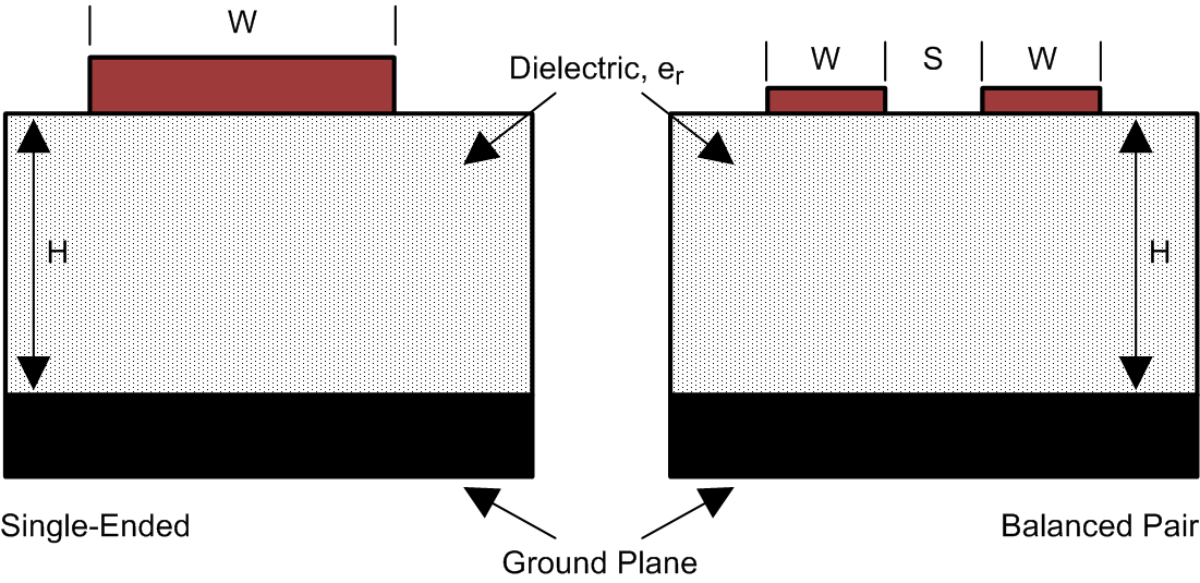
As per SLLD009, printed-circuit boards usually offer designers two transmission line options: Microstrip and stripline. Microstrips are traces on the outer layer of a PCB, as shown in Figure 23.
 Figure 23. Microstrip Topology
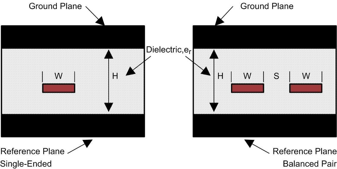
On the other hand, striplines are traces between two ground planes. Striplines are less prone to emissions and susceptibility problems because the reference planes effectively shield the embedded traces. However, from the standpoint of high-speed transmission, juxtaposing two planes creates additional capacitance. TI recommends routing LVDS signals on microstrip transmission lines, if possible. The PCB traces allow designers to specify the necessary tolerances for ZO based on the overall noise budget and reflection allowances. Footnotes 1(1), 2(2), and 3(3) provide formulas for ZO and tPD for differential and single-ended traces. (1) (2) (3)
 Figure 24. Stripline Topology
13.1.2 Dielectric Type and Board Construction
The speeds at which signals travel across the board dictates the choice of dielectric. FR-4, or equivalent, usually provides adequate performance for use with LVDS signals. If rise or fall times of TTL/CMOS signals are less than 500 ps, empirical results indicate that a material with a dielectric constant near 3.4, such as Rogers™ 4350 or Nelco N4000-13 is better suited. Once the designer chooses the dielectric, there are several parameters pertaining to the board construction that can affect performance. The following set of guidelines were developed experimentally through several designs involving LVDS devices:
- Copper weight: 15 g or 1/2 oz start, plated to 30 g or 1 oz
- All exposed circuitry should be solder-plated (60/40) to 7.62 μm or 0.0003 in (minimum).
- Copper plating should be 25.4 μm or 0.001 in (minimum) in plated-through-holes.
- Solder mask over bare copper with solder hot-air leveling
13.1.3 Recommended Stack Layout
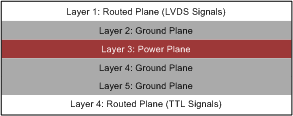
Following the choice of dielectrics and design specifications, you should decide how many levels to use in the stack. To reduce the TTL/CMOS to LVDS crosstalk, it is a good practice to have at least two separate signal planes as shown in Figure 25.
 Figure 25. Four-Layer PCB Board
NOTE
The separation between layers 2 and 3 should be 127 μm (0.005 in). By keeping the power and ground planes tightly coupled, the increased capacitance acts as a bypass for transients.
One of the most common stack configurations is the six-layer board, as shown in Figure 26.
 Figure 26. Six-Layer PCB Board
In this particular configuration, it is possible to isolate each signal layer from the power plane by at least one ground plane. The result is improved signal integrity; however, fabrication is more expensive. Using the 6-layer board is preferable, because it offers the layout designer more flexibility in varying the distance between signal layers and referenced planes, in addition to ensuring reference to a ground plane for signal layers 1 and 6.
13.1.4 Separation Between Traces
The separation between traces depends on several factors; however, the amount of coupling that can be tolerated usually dictates the actual separation. Low-noise coupling requires close coupling between the differential pair of an LVDS link to benefit from the electromagnetic field cancellation. The traces should be 100-Ω differential and thus coupled in the manner that best fits this requirement. In addition, differential pairs should have the same electrical length to ensure that they are balanced, thus minimizing problems with skew and signal reflection.
In the case of two adjacent single-ended traces, one should use the 3-W rule, which stipulates that the distance between two traces should be greater than two times the width of a single trace, or three times its width measured from trace center to trace center. This increased separation effectively reduces the potential for crosstalk. The same rule should be applied to the separation between adjacent LVDS differential pairs, whether the traces are edge-coupled or broad-side-coupled.
 Figure 27. 3-W Rule for Single-Ended and Differential Traces (Top View)
You should exercise caution when using autorouters, because they do not always account for all factors affecting crosstalk and signal reflection. For instance, it is best to avoid sharp 90° turns to prevent discontinuities in the signal path. Using successive 45° turns tends to minimize reflections.
13.1.5 Crosstalk and Ground Bounce Minimization
To reduce crosstalk, it is important to provide a return path to high-frequency currents that is as close as possible to its originating trace. A ground plane usually achieves this. Because the returning currents always choose the path of lowest inductance, they are most likely to return directly under the original trace, thus minimizing crosstalk. Lowering the area of the current loop lowers the potential for crosstalk. Traces kept as short as possible with an uninterrupted ground plane running beneath them emit the minimum amount of electromagnetic field strength. Discontinuities in the ground plane increase the return path inductance and should be avoided.
13.2 Layout Example
At least two or three times the width of an individual trace should separate single-ended traces and differential pairs to minimize the potential for crosstalk. Single-ended traces that run in parallel for less than the wavelength of the rise or fall times usually have negligible crosstalk. Increase the spacing between signal paths for long parallel runs to reduce crosstalk. Boards with limited real estate can benefit from the staggered trace layout, as shown in Figure 28.
 Figure 28. Staggered Trace Layout
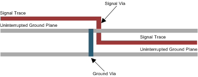
This configuration lays out alternating signal traces on different layers; thus, the horizontal separation between traces can be less than 2 or 3 times the width of individual traces. To ensure continuity in the ground signal path, TI recommends having an adjacent ground via for every signal via, as shown in Figure 29. Note that vias create additional capacitance. For example, a typical via has a lumped capacitance effect of 1/2 pF to 1 pF in FR4.
 Figure 29. Ground Via Location (Side View)
Short and low-impedance connection of the device ground pins to the PCB ground plane reduces ground bounce. Holes and cutouts in the ground planes can adversely affect current return paths if they create discontinuities that increase returning current loop areas.
To minimize EMI problems, TI recommends avoiding discontinuities below a trace (for example, holes, slits, and so on) and keeping traces as short as possible. Zoning the board wisely by placing all similar functions in the same area, as opposed to mixing them together, helps reduce susceptibility issues.