JAJSCH4 September 2016 SN75LVPE801
PRODUCTION DATA.
- 1 特長
- 2 アプリケーション
- 3 概要
- 4 改訂履歴
- 5 概要(続き)
- 6 Pin Configuration and Functions
- 7 Specifications
- 8 Parameter Measurement Information
- 9 Detailed Description
- 10Applications and Implementation
- 11Power Supply Recommendations
- 12Layout
- 13デバイスおよびドキュメントのサポート
- 14メカニカル、パッケージ、および注文情報
10 Applications and Implementation
NOTE
Information in the following applications sections is not part of the TI component specification, and TI does not warrant its accuracy or completeness. TI’s customers are responsible for determining suitability of components for their purposes. Customers should validate and test their design implementation to confirm system functionality.
10.1 Application Information
The SN75LVPE801 can be used for SATA applications as well as SATA Express applications. The device supports SATA Gen1, Gen2, and Gen3 applications with data rates from 1.5 to 8 Gbps. The built-in equalization circuits provide up to 16 dB of equalization at 4 GHz. This equalization can support SATA GEN2 (3 Gbps) applications over up to 50 inches of FR-4 material. The same 16 dB equalizer is suited to SATA Gen3 (8 Gbps) applications up to 40 inches of FR4.
In addition to SATA applications, the SN75LVPE801 can support SATA Express applications. SATA Express provides a standardized interface to support both SATA (Gen1, Gen2, and Gen3) and PCI Express (PCIe 1.0, 2.0 and 3.0).
All applications of the SN75LVPE801 share some common applications issues. For example, power supply filtering, board layout, and equalization performance with varying interconnect losses. Other applications issues are specific, such as implementing receiver detection for SATA Express applications. The Typical Application examples demonstrate common implementations of the SN75LVPE801 supporting SATA, as well as SATA Express applications.
10.2 Typical SATA Applications
10.2.1 Design Requirements
| DESIGN PARAMETERS | VALUE |
|---|---|
| SATA Signaling Rate | 1.5 - 6.0 Gbps |
| AC Coupling Capacitance | 10 nF |
| Interconnect Characteristic Impedance | 100 Ohms |
| Interconnect Length | Up to 50" FR4 for SATA Gen2 Up to 40" FR4 for SATA Gen3 |
| Termination Resistance | 100 Ohms differential integrated into TX and RX |
10.2.2 Detailed Design Procedure
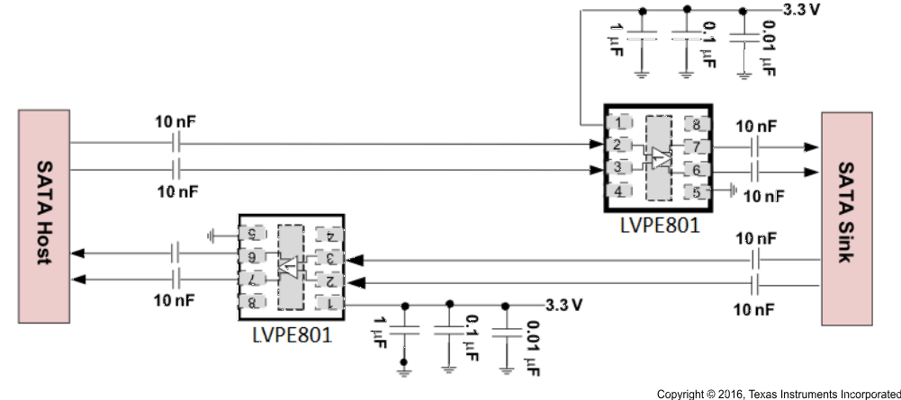
Figure 11 shows a typical SATA Application. The SATA host, which may be a notebook or desktop, communicates with a SATA sink, which could be a SSD mass storage device. The SATA host and sink communicate over a backplane differential pair, or a SATA cable. When using the SN75LVPE801 as an equalizer/redriver, the designer would optimally place the SN75LVPE801 close to the end of the interconnect. The SN75LVPE801 provides up to 16 dB of equalization, and up to 1.2 dB of de-emphasis. Placing the SN75LVPE801 close to the end of the interconnect allows the device equalizer to address the majority of the high frequency losses introduced in the channel.
Ensure that the channel loss for the interconnect material and length is matched reasonably well to the selectable equalization and de-emphasis settings available on the SN75LVPE801. The table above provides an estimate of the amount of FR4 material that could be used as a function of the signal rate. In any case, channel modeling would be prudent to ensure that the SATA host, interconnect, SATA equalizer/re-driver, and SATA Sink can establish and maintain a low BER link.
The AC coupling capacitors of 10 nF are chosen to comply with the SATA standard (< 12 nF)
Often a designer may not be sure whether a signal conditioning device like the SN75LVPE801 is needed in their specific application. The SN75LVPE801 allows the user to take the guess work of using a signal conditioning device in a SATA link. With the SN75LVPE801 the designer has the option to use or remove the device based on signal conditioning needs. Figure 12 shows guidelines that could be used to allow in situ testing when a board is available. The designer would start with 0 Ω resistors in place to determine if the eye quality at the end of the link is satisfactory. If the eye opening is not sufficient, the 0 Ω resistors could be replaced with the SN75LVPE801.
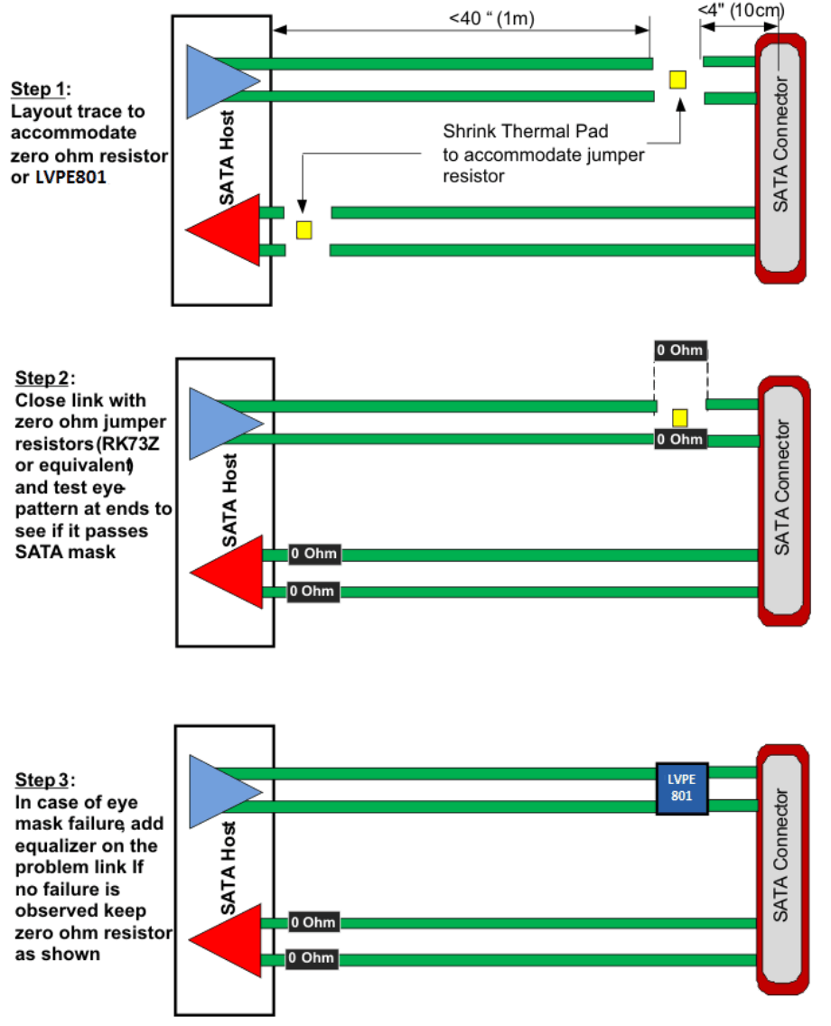 Figure 12. Implementation Guideline
To demonstrate the effectiveness of the SN75LVPE801 signal conditioning for varied configurations that may be encountered, Figure 13 is used as a reference. A Gen3, 6 Gbps SATA host communicates with a sink located at point B. The host and sink are separated by “X+Y” inches, where X represents the distance between the host and the SN75LVPE801, while Y represents the distance between the SN75LVPE801 and the sink. The Application Curves are for a 6-Gbps K28.5 pattern, with VCC = 3.3 V and at an ambient temperature of 25°C.
 Figure 13. Test Points
10.2.3 Application Curves
All graphs at 6 Gbps
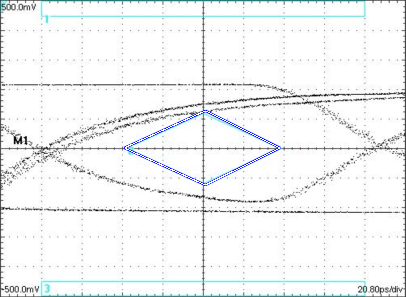
| DE = 1 | EQ = 0 |
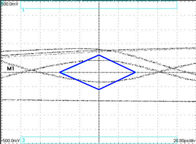
| DE = 1 | EQ = 0 |
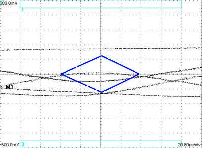
| DE = 1 | EQ = 0 |
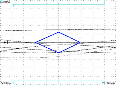
| DE = 1 | EQ = 1 |
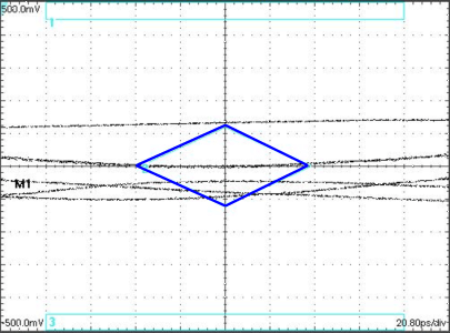
| DE = 1 | EQ = 1 |
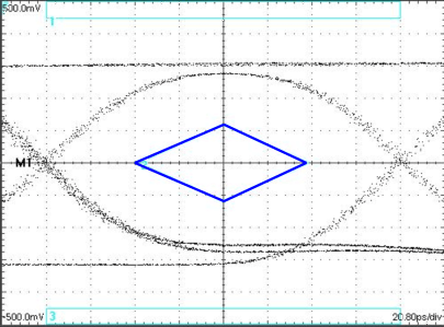
| DE = 1 | EQ = 0 |
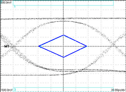
| DE = 1 | EQ = 0 |
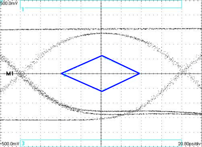
| DE = 1 | EQ = 0 |
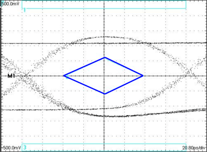
| DE = 1 | EQ = 1 |
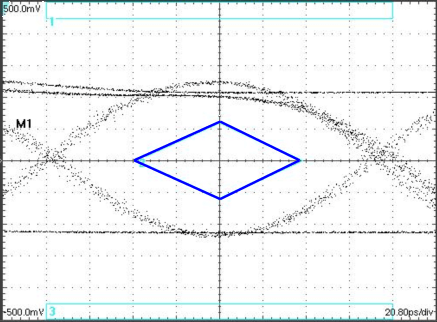
| DE = 1 | EQ = 1 |
10.2.4 SATA Express Applications
 Figure 24. SN75LVPE801 SATA Express Reference Schematic
 EQ: 8 dB when Floated, DE: 0 dB when Floated
10.2.4.1 Design Requirements
| DESIGN PARAMETERS | VALUE |
|---|---|
| SATA Express Signaling Rate | 1.5 - 8.0 Gbps |
| AC Coupling Capacitance | 200 - 220 nF |
| Interconnect Characteristic Impedance | 100 Ω |
| Interconnect Length | Up to 50" FR4 for SATA Gen2 Up to 40" FR4 for SATA Gen3 |
| Receiver pull-down terminations | 330 Ω |
| Termination Resistance | 100 Ohms differential integrated into TX and RX |
10.2.4.2 Detailed Design Procedure
Figure 24 is a reference schematic of a SATAe implementation using the SN75LVPE801. With a SATAe design, both SATA and PCI Express must be supported. SATAe supports both cabled and direct connections. Using a cabled application as an example, the SATAe power connector includes an Interface Detect (IFDet, power connector pin P4) signal that indicates whether a SATA client or a PCIe client is connected.
When the SATAe host determines that a PCIe client is connected, the SATAe host performs receiver detection. Receiver detection determines the presence of a client by detecting the load impedance. The transmitter performs a common mode voltage shift, and measures the rate at which the voltage at the transmitter output changes. The rate of change indicates if a client is present (fast charging when a low impedance load is present, or slow charging when the load is open or high impedance). With the implementation in Figure 24, 330-Ω pulldowns have been inserted between the host and the SN75LVPE801. The pulldown resistors indicate to the host that a client is present. While an actual client would be expected to have an active load of 50 Ω single ended, the 330 Ω is chosen here to meet two requirements. The 330 Ω is low enough to force the SATAe host to decide that a receiver is present, while also high enough to only marginally affect the load when the SN75LVPE801 is active, and presenting a 50-Ω load. With the 50 Ω and 330 Ω are both present, the parallel combination of 43 Ω is satisfactory for most applications.
Assuming that the SATAe host has detected (via IFDet) that a SATA client is present, the SATAe host communicates with the client via the SN75LVPE801. The SATA standard does not have a receiver detection mode as is present in PCIe. A SATA host does use OOB signaling to communicate identification information. The SN75LVPE801 incorporates an OOB detector in order to support OOB signaling through the device. The OOB detector drives a squelch circuit on the SN75LVPE801 output transmitter. (See OOB/Squelch for more details on the OOB/Squelch circuitry.)
Returning again to Figure 24, we see 200-nF AC coupling capacitors on the device or client side of the interface. These capacitors allow interfacing to both SATA and PCIe clients. In the case of a PCIe client, the 200 nF is within the acceptable range for all PCIe devices. When a SATA client is present, the 200 nF capacitor has little effect on the overall link, as it appears in series with the 12-nF (max) AC coupling capacitor incorporated into the SATA client. The 200 nF in series with the 12 nF presents an effective capacitance of 11.3 nF, as expected less than the 12-nF maximum permitted.
The physical placement of the resistors on the high-speed transmission lines can be made as not to create a stub on the transmission line by using resistors with the 0201 package size, an example is provided in Figure 25.
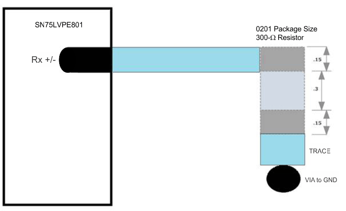 Figure 25. Resistor Placement to Avoid Stub (All Dimensions in mm)
10.2.4.3 Application Curve
Eye-diagrams were taken on the SN75LVPE801 configured as in Figure 24 above. Testing was performed at a PCIe 3.0 speed of 8Gbps.
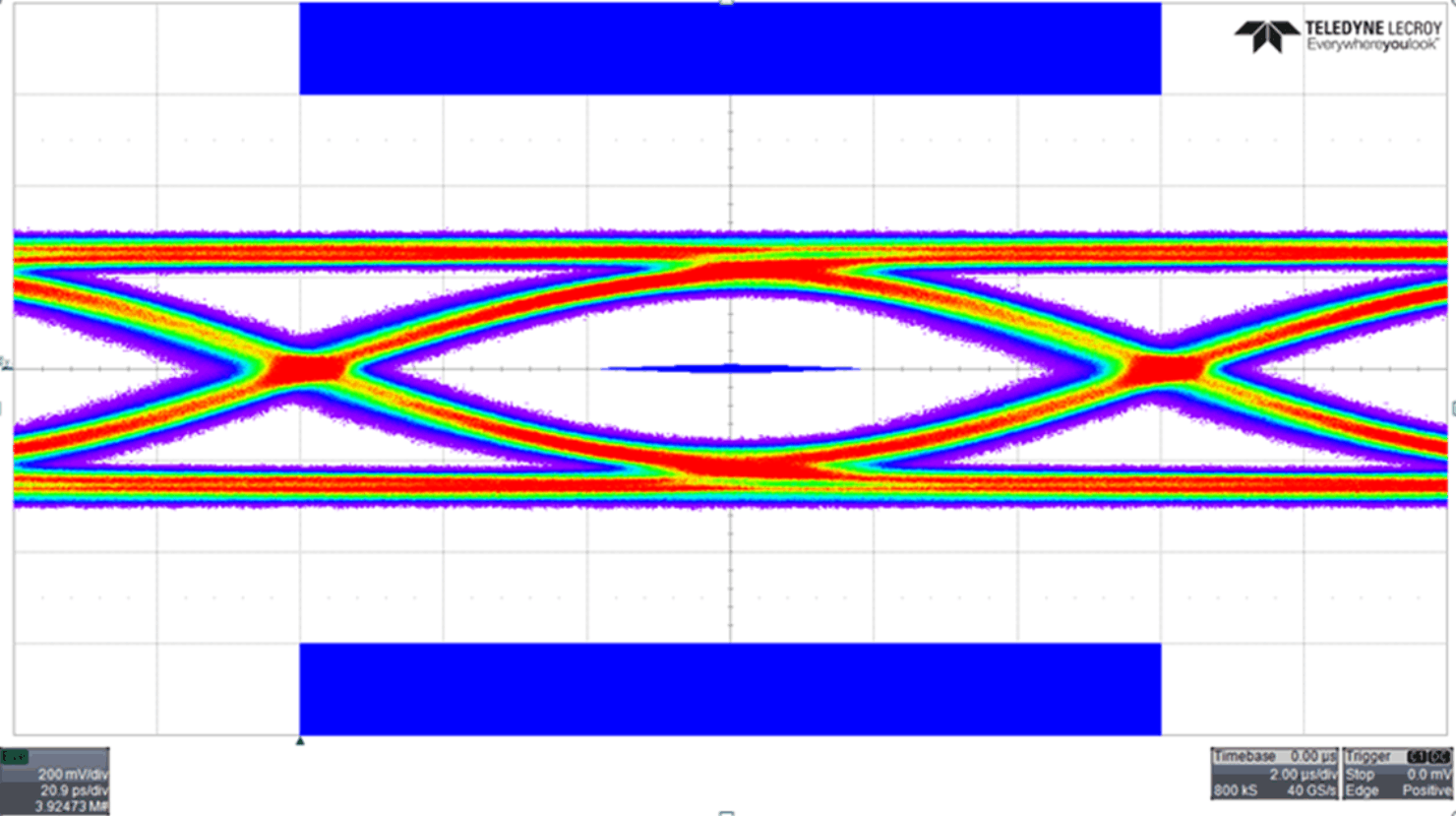 Figure 26. SN75LVPE801 8-Gbps Eye-Diagram
10.2.5 PCIe Applications
PCIe-only applications are implemented in a manner very similar to SATA Express applications as covered in Detailed Design Procedure. Looking at Figure 27, and comparing it to the SATA Express application in Figure 24, a single change is noted. For PCIe applications the 220 nF AC-coupling capacitors on the Host-to-Device link are relocated from the Device side of the connector to the Host side. No other changes are required.
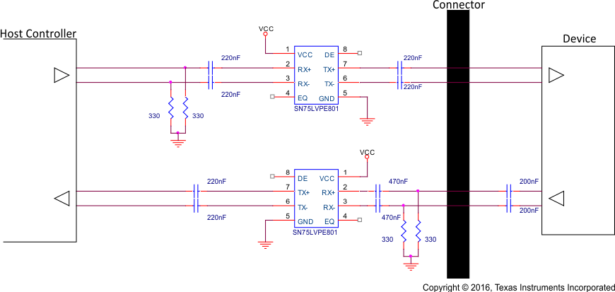 Figure 27. SN75LVPE801 PCI-Express Reference Schematic
EQ: 7 dB when Floated, DE: 0 dB when Floated