JAJSCH4 September   2016 SN75LVPE801

PRODUCTION DATA.  

  1. 特長
  2. アプリケーション
  3. 概要
  4. 改訂履歴
  5. 概要(続き)
  6. Pin Configuration and Functions
  7. Specifications
    1. 7.1 Absolute Maximum Ratings
    2. 7.2 ESD Ratings
    3. 7.3 Recommended Operating Conditions
    4. 7.4 Thermal Information
    5. 7.5 Electrical Characteristics
    6. 7.6 Timing Requirements
    7. 7.7 Typical Characteristics
  8. Parameter Measurement Information
  9. Detailed Description
    1. 9.1 Overview
    2. 9.2 Functional Block Diagram
    3. 9.3 Feature Description
      1. 9.3.1  SATA Express
      2. 9.3.2  Receiver Termination
      3. 9.3.3  Receiver Internal Bias
      4. 9.3.4  Receiver Equalization
      5. 9.3.5  OOB/Squelch
      6. 9.3.6  Auto Low Power
      7. 9.3.7  Transmitter Output Signal
      8. 9.3.8  Transmitter Common Mode
      9. 9.3.9  De-Emphasis
      10. 9.3.10 Transmitter Termination
    4. 9.4 Device Functional Modes
      1. 9.4.1 Active
      2. 9.4.2 Squelch
      3. 9.4.3 Auto Low Power
  10. 10Applications and Implementation
    1. 10.1 Application Information
    2. 10.2 Typical SATA Applications
      1. 10.2.1 Design Requirements
      2. 10.2.2 Detailed Design Procedure
      3. 10.2.3 Application Curves
      4. 10.2.4 SATA Express Applications
        1. 10.2.4.1 Design Requirements
        2. 10.2.4.2 Detailed Design Procedure
        3. 10.2.4.3 Application Curve
      5. 10.2.5 PCIe Applications
  11. 11Power Supply Recommendations
  12. 12Layout
    1. 12.1 Layout Guidelines
      1. 12.1.1 Return Current and Plane References
      2. 12.1.2 Split Planes - What to Avoid
      3. 12.1.3 Avoiding Crosstalk
    2. 12.2 Layout Example
  13. 13デバイスおよびドキュメントのサポート
    1. 13.1 デバイス・サポート
      1. 13.1.1 Third-Party Products Disclaimer
    2. 13.2 ドキュメントの更新通知を受け取る方法
    3. 13.3 コミュニティ・リソース
    4. 13.4 商標
    5. 13.5 静電気放電に関する注意事項
    6. 13.6 Glossary
  14. 14メカニカル、パッケージ、および注文情報

パッケージ・オプション

メカニカル・データ(パッケージ|ピン)
サーマルパッド・メカニカル・データ
発注情報

6 Pin Configuration and Functions

DRF Package
8-Pin WSON
Top View
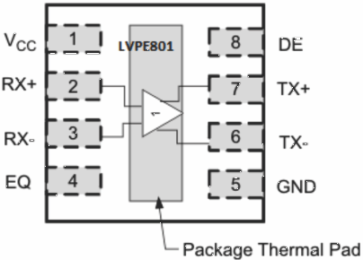
SN75LVPE801 po_sllsel6.gif

Pin Functions

PIN TYPE(1) DESCRIPTION
NAME NO.
HIGH SPEED DIFFERENTIAL I/O
RX+ 2 I Noninverting and inverting CML differential inputs. These pins are tied to an internal voltage bias by dual termination resistor circuit.
RX– 3 I
TX+ 7 O Noninverting and inverting VML differential outputs. These pins are tied to an internal voltage bias by dual termination resistor circuit.
TX– 6 O
CONTROL PINS
EQ 4 I Selects equalization settings per Table 1. Internally tied to GND.
DE 8 I Selects de-emphasis settings per Table 1. Internally tied to GND.
POWER
VCC 1 P Positive supply must be 3.3 V ±10%
GND 5 G Supply ground
(1) G = Ground, I = Input, O = Output, P = Power