JAJSIU0C April   2020  – September 2023 TAS5441-Q1

PRODUCTION DATA  

  1.   1
  2. 特長
  3. アプリケーション
  4. 概要
  5. Revision History
  6. Pin Configuration and Functions
  7. Specifications
    1. 6.1 Absolute Maximum Ratings
    2. 6.2 ESD Ratings
    3. 6.3 Recommended Operating Conditions
    4. 6.4 Thermal Information
    5. 6.5 Electrical Characteristics
    6. 6.6 Timing Requirements for I2C Interface Signals
    7. 6.7 Typical Characteristics
  8. Detailed Description
    1. 7.1 Overview
    2. 7.2 Functional Block Diagram
    3. 7.3 Feature Description
      1. 7.3.1 Analog Audio Input and Preamplifier
      2. 7.3.2 Pulse-Width Modulator (PWM)
      3. 7.3.3 Gate Drive
      4. 7.3.4 Power FETs
      5. 7.3.5 Load Diagnostics
        1. 7.3.5.1 Load Diagnostics Sequence
        2. 7.3.5.2 Faults During Load Diagnostics
      6. 7.3.6 Protection and Monitoring
      7. 7.3.7 I2C Serial Communication Bus
        1. 7.3.7.1 I2C Bus Protocol
        2. 7.3.7.2 Random Write
        3. 7.3.7.3 Random Read
        4. 7.3.7.4 Sequential Read
    4. 7.4 Device Functional Modes
      1. 7.4.1 Hardware Control Pins
      2. 7.4.2 EMI Considerations
      3. 7.4.3 Operating Modes and Faults
    5. 7.5 Register Maps
      1. 7.5.1 I2C Address Register Definitions
  9. Application and Implementation
    1. 8.1 Application Information
    2. 8.2 Typical Application
      1. 8.2.1 Design Requirements
        1. 8.2.1.1 Amplifier Output Filtering
        2. 8.2.1.2 Amplifier Output Snubbers
        3. 8.2.1.3 Bootstrap Capacitors
        4. 8.2.1.4 Analog Audio Input Filter
      2. 8.2.2 Detailed Design Procedure
        1. 8.2.2.1 Unused Pin Connections
          1. 8.2.2.1.1 MUTE Pin
          2. 8.2.2.1.2 STANDBY Pin
          3. 8.2.2.1.3 I2C Pins (SDA and SCL)
          4. 8.2.2.1.4 Terminating Unused Outputs
          5. 8.2.2.1.5 Using a Single-Ended Audio Input
      3. 8.2.3 Application Curves
  10. Layout
    1. 9.1 Layout Guidelines
    2. 9.2 Layout Examples
      1. 9.2.1 Top Layer
      2. 9.2.2 Second Layer – Signal Layer
  11. 10Device and Documentation Support
    1. 10.1 Device Support
      1. 10.1.1 サード・パーティ製品に関する免責事項
    2. 10.2 Documentation Support
      1. 10.2.1 Related Documentation
    3. 10.3 ドキュメントの更新通知を受け取る方法
    4. 10.4 サポート・リソース
    5. 10.5 Trademarks
    6. 10.6 静電気放電に関する注意事項
    7. 10.7 用語集
  12. 11Mechanical, Packaging, and Orderable Information

パッケージ・オプション

メカニカル・データ(パッケージ|ピン)
サーマルパッド・メカニカル・データ
発注情報

Pulse-Width Modulator (PWM)

The PWM converts the analog signal from the preamplifier into a switched signal of varying duty cycle. This is the critical stage that defines the class-D architecture. In the TAS5441-Q1, the modulator is an advanced design with high bandwidth, low noise, low distortion, and excellent stability.

The pulse-width modulation scheme allows increased efficiency at low power. Each output is switching from 0 V to PVDD. The OUTP and OUTN pins are in phase with each other with no input so that there is little or no current in the speaker. The duty cycle of OUTP is greater than 50% and the duty cycle OUTN is less than 50% for positive output voltages. The duty cycle of OUTN is greater than 50% and the duty cycle of OUTP is less than 50% for negative output voltages. The voltage across the load is at 0 V through most of the switching period, reducing power loss.
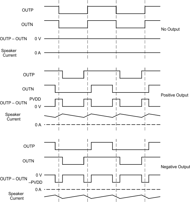
GUID-E2C962F4-5233-427D-BAB7-7DF9579B141F-low.gifFigure 7-1 BD Mode Modulation