JAJSI51A May   2019  – January 2023 TAS5825P

PRODUCTION DATA  

  1. 特長
  2. アプリケーション
  3. 概要
  4. Revision History
  5. Device Comparison Table
  6. Pin Configuration and Functions
  7. Specifications
    1. 7.1 Absolute Maximum Ratings
    2. 7.2 ESD Ratings
    3. 7.3 Recommended Operating Conditions
    4. 7.4 Thermal Information
    5. 7.5 Electrical Characteristics
    6. 7.6 Timing Requirements
    7. 7.7 Typical Characteristics
      1. 7.7.1 Bridge Tied Load (BTL) Configuration Curves with Hybrid Modulation
      2. 7.7.2 Parallel Bridge Tied Load (PBTL) Configuration With Hybrid Modulation
      3. 7.7.3 Bridge Tied Load (BTL) Configuration Curves with BD Modulation
      4. 7.7.4 Parallel Bridge Tied Load (PBTL) Configuration With BD Modulation
  8. Parameter Measurement Information
  9. Detailed Description
    1. 9.1 Overview
    2. 9.2 Functional Block Diagram
    3. 9.3 Feature Description
      1. 9.3.1 Power Supplies
      2. 9.3.2 Device Clocking
      3. 9.3.3 Serial Audio Port – Clock Rates
      4. 9.3.4 Clock Halt Auto-Recovery
      5. 9.3.5 Sample Rate on the Fly Change
      6. 9.3.6 Serial Audio Port - Data Formats and Bit Depths
      7. 9.3.7 Digital Audio Processing
      8. 9.3.8 Class-D Audio Amplifier
        1. 9.3.8.1 Speaker Amplifier Gain Select
        2. 9.3.8.2 Class D Loop Bandwidth and Switching Frequency Setting
    4. 9.4 Device Functional Modes
      1. 9.4.1 Software Control
      2. 9.4.2 Speaker Amplifier Operating Modes
        1. 9.4.2.1 BTL Mode
        2. 9.4.2.2 PBTL Mode
      3. 9.4.3 Low EMI Modes
        1. 9.4.3.1 Spread Spectrum
        2. 9.4.3.2 Channel to Channel Phase Shift
        3. 9.4.3.3 Multi-Devices PWM Phase Synchronization
          1. 9.4.3.3.1 Phase Synchronization With I2S Clock In Startup Phase
          2. 9.4.3.3.2 Phase Synchronization With GPIO
      4. 9.4.4 Thermal Foldback
      5. 9.4.5 Device State Control
      6. 9.4.6 Device Modulation
        1. 9.4.6.1 BD Modulation
        2. 9.4.6.2 1SPW Modulation
        3. 9.4.6.3 Hybrid Modulation
    5. 9.5 Programming and Control
      1. 9.5.1 I2 C Serial Communication Bus
      2. 9.5.2 I2 C Peripheral Address
        1. 9.5.2.1 Random Write
        2. 9.5.2.2 Sequential Write
        3. 9.5.2.3 Random Read
        4. 9.5.2.4 Sequential Read
        5. 9.5.2.5 DSP Memory Book, Page and BQ update
        6. 9.5.2.6 Checksum
          1. 9.5.2.6.1 Cyclic Redundancy Check (CRC) Checksum
          2. 9.5.2.6.2 Exclusive or (XOR) Checksum
      3. 9.5.3 Control via Software
        1. 9.5.3.1 Startup Procedures
        2. 9.5.3.2 Shutdown Procedures
        3. 9.5.3.3 Protection and Monitoring
          1. 9.5.3.3.1 Overcurrent Limit (Cycle-By-Cycle)
          2. 9.5.3.3.2 Overcurrent Shutdown (OCSD)
          3. 9.5.3.3.3 DC Detect
    6. 9.6 Register Maps
      1. 9.6.1 CONTROL PORT Registers
  10. 10Application and Implementation
    1. 10.1 Application Information
      1. 10.1.1 Bootstrap Capacitors
      2. 10.1.2 Inductor Selections
      3. 10.1.3 Power Supply Decoupling
      4. 10.1.4 Output EMI Filtering
    2. 10.2 Typical Applications
      1. 10.2.1 2.0 (Stereo BTL) System
      2. 10.2.2 79
      3. 10.2.3 Design Requirements
      4. 10.2.4 Detailed Design procedures
        1. 10.2.4.1 Step One: Hardware Integration
        2. 10.2.4.2 Step Two: Hardware Integration
        3. 10.2.4.3 Step Three: Software Integration
      5. 10.2.5 Application Curves
      6. 10.2.6 MONO (PBTL) Systems
      7. 10.2.7 Application Curves
    3. 10.3 Power Supply Recommendations
      1. 10.3.1 DVDD Supply
      2. 10.3.2 PVDD Supply
    4. 10.4 Layout
      1. 10.4.1 Layout Guidelines
        1. 10.4.1.1 General Guidelines for Audio Amplifiers
        2. 10.4.1.2 Importance of PVDD Bypass Capacitor Placement on PVDD Network
        3. 10.4.1.3 Optimizing Thermal Performance
          1. 10.4.1.3.1 Device, Copper, and Component Layout
          2. 10.4.1.3.2 Stencil Pattern
            1. 10.4.1.3.2.1 PCB footprint and Via Arrangement
            2. 10.4.1.3.2.2 Solder Stencil
      2. 10.4.2 Layout Example
  11. 11Device and Documentation Support
    1. 11.1 Device Support
      1. 11.1.1 Device Nomenclature
      2. 11.1.2 Development Support
    2. 11.2 Receiving Notification of Documentation Updates
    3. 11.3 サポート・リソース
    4. 11.4 Trademarks
    5. 11.5 静電気放電に関する注意事項
    6. 11.6 用語集
  12. 12Mechanical, Packaging, and Orderable Information

パッケージ・オプション

メカニカル・データ(パッケージ|ピン)
サーマルパッド・メカニカル・データ
発注情報

概要

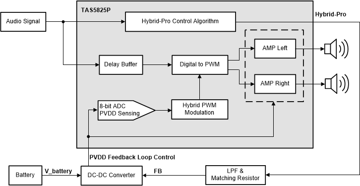
TAS5825P は、先進の Hybrid-Pro アルゴリズムを備えたステレオ、高効率、閉ループ Class-D オーディオ・アンプであり、クリッピング歪みを発生させずにシステム効率を高めることができます。

通常、オーディオ・アンプの電源電圧 (PVDD) は DC-DC コンバータで供給されます。固定 PVDD に比べて、オーディオ信号に基づいて変化する可変 PVDD は、大幅に効率を向上させ、アイドル電流を低減し、発熱を低減します。

TAS5825P の強力なオーディオ DSP コアは、Hybrid-Pro と呼ぶ独自のアルゴリズムを実装しています。Hybrid-Pro アルゴリズムは、予測されるオーディオ電力の需要を検出し、Hybrid-Pro フィードバック・ピン (HPFB) により、前段の DC-DC コンバータに PWM 制御信号を出力します。TAS5825P は、オーディオ信号を先読みしてオーディオ・クリッピング歪みを防止するために最大 4ms の遅延バッファをサポートしています。各種の実験において TAS5825P は、連続的に音楽を再生しながら、1S および 2S バッテリの動作時間を 50% 以上延長しました。

製品情報(1)
部品番号パッケージ本体サイズ (公称)
TAS5825PVQFN (32) RHB5.00mm × 5.00mm
利用可能なパッケージについては、このデータシートの末尾にある注文情報を参照してください。
GUID-A1A7D99F-8D5B-4AA7-AB10-720D6E772796-low.gif