JAJSHZ2C January 2014 – September 2019 TCA5013
PRODUCTION DATA.
- 1 特長
- 2 アプリケーション
- 3 概要
- 4 改訂履歴
- 5 Pin Configuration and Functions
-
6 Specifications
- 6.1 Absolute Maximum Ratings
- 6.2 Handling Ratings
- 6.3 Recommended Operating Conditions
- 6.4 Thermal Information
- 6.5 Electrical Characteristics—Power Supply and ESD
- 6.6 Electrical Characteristics—Card VCC
- 6.7 Electrical Characteristics—Card RST
- 6.8 Electrical Characteristics—Card CLK
- 6.9 Electrical Characteristics—Card Interface IO, C4 and C8
- 6.10 Electrical Characteristics—PRES
- 6.11 Electrical Characteristics—IOMC1 and IOMC2
- 6.12 Electrical Characteristics—CLKIN1 and CLKIN2
- 6.13 Electrical Characteristics—A0 and SHDN
- 6.14 Electrical Characteristics—INT
- 6.15 Electrical Characteristics—GPIO
- 6.16 Electrical Characteristics—SDA and SCL
- 6.17 Electrical Characteristics—Fault Condition Detection
- 6.18 I2C Interface Timing Requirements
- 6.19 I2C Interface Timing Characteristics
- 6.20 Synchronous Type 1 Card Activation Timing Characteristics
- 6.21 Synchronous Type 2 Card Activation Timing Characteristics
- 6.22 Card Deactivation Timing Characteristics
- 6.23 Typical Characteristics
- 7 Parameter Measurement Information
-
8 Detailed Description
- 8.1 Overview
- 8.2 Functional Block Diagram
- 8.3 Feature Description
- 8.4 Device Functional Modes
- 8.5 Programming
- 8.6 Register Maps
- 9 Application and Implementation
- 10Power Supply Recommendations
- 11Layout
- 12デバイスおよびドキュメントのサポート
- 13メカニカル、パッケージ、および注文情報
8.4.4.3 Synchronous Type 2 Operating Mode
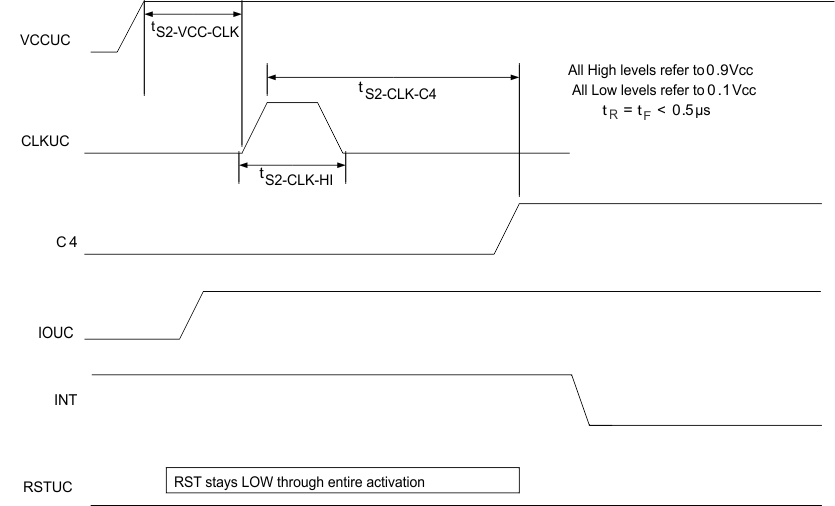
Synchronous type 2 operating mode is only supported on the user card interface. To enter synchronous operating mode, the user card interface goes through the synchronous type 2 activation sequence. Figure 5 shows the synchronous type 2 activation sequence.
CLKIN1 shall be low before the synchronous type 2 activation sequence is initiated. The following bit settings are required to initiate a synchronous type 1 activation sequence.
- ACTIVATION_TYPE (bit [6]; Reg 0x09) = 1
- CARD_TYPE (bit [7]; Reg 0x09) = 1
- START_SYNC (bit [0]; Reg 0x09) = 1
 Figure 5. Synchronous Type 2 Activation Sequence
 Once synchronous type 2 activation has been initiated, the following sequence of events occur on the user card interface:
- VCCUC, RSTUC, CLKUC, C4, C8 and IOUC are all default low.
- VCC is applied to the VCCUC pin per the SET_VCC_UC bit (bit[7:6]; Reg 0x01).
- A single pulse is applied to CLKUC per the tS2-CLK-HI timing defined in Table 3.
- The C4 line is held low through the VCC ramp.
- The C4 line is released high per the tS2-CLK-C4 timing defined in Table 3.
- After C4 is released CLKUC is controlled by clock settings register (Reg 0x02).
- After VCC is stable, the IOUC line is pulled up to VCC.
- After VCC is stable, C8 reflects value in bit [4] Reg 0x09.
- IOUC is connected to IOMC1 if IO_EN_UC bit (bit[5] Reg 0x01) is set to 1.
- INT_SYNC_COMPLETE bit (Bit[1]; REG 0x41) is set and the INT line is asserted low.
- IOMC1 shall stay pulled up to VDDI , that is, IOMC1 shall not be pulled low until INT is asserted.
- CLKIN1 shall toggle only after INT is asserted.
- RSTUC is controllable by I2C after INT is asserted.
Table 3. Synchronous Type 2 Card Activation Timing Characteristics
| MIN | TYP | MAX | UNIT | |
|---|---|---|---|---|
| tS2-VCC-CLK | 5 | 20 | µs | |
| tS2-CLK-C4 | 14 | 18 | 22 | µs |
| tS2-CLK-HI | 7 | 9 | 11 | µs |