JAJSHZ2C January 2014 – September 2019 TCA5013
PRODUCTION DATA.
- 1 特長
- 2 アプリケーション
- 3 概要
- 4 改訂履歴
- 5 Pin Configuration and Functions
-
6 Specifications
- 6.1 Absolute Maximum Ratings
- 6.2 Handling Ratings
- 6.3 Recommended Operating Conditions
- 6.4 Thermal Information
- 6.5 Electrical Characteristics—Power Supply and ESD
- 6.6 Electrical Characteristics—Card VCC
- 6.7 Electrical Characteristics—Card RST
- 6.8 Electrical Characteristics—Card CLK
- 6.9 Electrical Characteristics—Card Interface IO, C4 and C8
- 6.10 Electrical Characteristics—PRES
- 6.11 Electrical Characteristics—IOMC1 and IOMC2
- 6.12 Electrical Characteristics—CLKIN1 and CLKIN2
- 6.13 Electrical Characteristics—A0 and SHDN
- 6.14 Electrical Characteristics—INT
- 6.15 Electrical Characteristics—GPIO
- 6.16 Electrical Characteristics—SDA and SCL
- 6.17 Electrical Characteristics—Fault Condition Detection
- 6.18 I2C Interface Timing Requirements
- 6.19 I2C Interface Timing Characteristics
- 6.20 Synchronous Type 1 Card Activation Timing Characteristics
- 6.21 Synchronous Type 2 Card Activation Timing Characteristics
- 6.22 Card Deactivation Timing Characteristics
- 6.23 Typical Characteristics
- 7 Parameter Measurement Information
-
8 Detailed Description
- 8.1 Overview
- 8.2 Functional Block Diagram
- 8.3 Feature Description
- 8.4 Device Functional Modes
- 8.5 Programming
- 8.6 Register Maps
- 9 Application and Implementation
- 10Power Supply Recommendations
- 11Layout
- 12デバイスおよびドキュメントのサポート
- 13メカニカル、パッケージ、および注文情報
8.4.4.5 Asynchronous Operating Mode
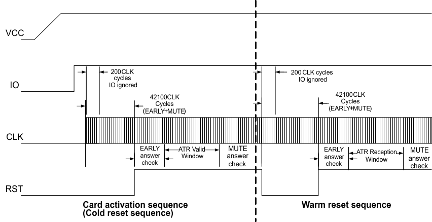
Asynchronous operating mode is supported on all card interfaces. To enter asynchronous operating mode, the user card interface goes through the asynchronous activation sequence. Figure 6 shows the asynchronous activation sequence. CLKIN1 shall be toggling before the asynchronous activation sequence is initiated. The asynchronous activation sequence is initiated by setting the START_ASYNC bit (bit[0]) of the card interface settings register (Reg 0x01 for User card, Reg 0x11 for SAM1, Reg 0x21 for SAM1, Reg 0x31 for SAM3) to ‘1’.
Once asynchronous activation has been initiated, the following sequence of events takes place on the card interface:
- VCC, RST, CLK, C4, C8 and IO are all default low.
- VCC is applied to the VCC pin per the SET_VCC bits (bit [7:6] of card interface settings register).
- After VCC is stable, the IO line is pulled up to VCC.
- After VCC is stable C4 and C8 reflect the value in their corresponding I2C register bits (bit[5] and bit[4]; Reg 0x09).
- IO is connected to IOMC if IO_EN bit (bit[5] of card interface settings register) is set to 1.
- The CLK line starts to oscillate based on the card clock settings register. Any change on the IO line during the first 200 card clock cycles on the CLK pin is ignored.
- After the first 42100 CLK cycles, the RST line is driven high.
- If there is a high to low transition on the IO line before RST is high, the EARLY bit (bit[6]) and MUTE bit (bit[5]) of the card interface status register (Reg 0x00 for user card, Reg 0x10 for SAM1, Reg 0x20 for SAM2 and Reg 0x30 for SAM3) is set and the INT pin is asserted low.
- After RST is high, an internal counter starts counting CLK cycles. If there is a high to low transition on IO pin before the internal counter reaches the value defined by in the EARLY_COUNT_HI register (Reg 0x03 for user card, Reg 0x13 for SAM1, Reg 0x23 for SAM2, Reg 0x33 for SAM3) and EARLY_ COUNT_LO Register (Reg 0x04 for user card, Reg 0x14 for SAM1, Reg 0x24 for SAM2, Reg 0x34 for SAM3) then the EARLY bit in the card interface status register is set and INT is asserted.
- If the internal counter reaches the value defined by MUTE_COUNT_HI register (Reg 0x05 for user card, Reg 0x15 for SAM1, Reg 0x25 for SAM2, Reg 0x35 for SAM3) and MUTE_COUNT_LO (Reg 0x06 for user card, Reg 0x16 for SAM1, Reg 0x26 for SAM2, Reg 0x36 for SAM3) registers without a high to low transition on the IO line, then the MUTE bit in the card interface status registers is set and INT pin is asserted low.
If the first high to low transition on IO pin happens very close to the clock edges (within ~10 ns) that defines the ATR VALID window (see Figure 6), the TCA5013 response would be non-deterministic, that is, it may not be able to identify whether the transition happened before or after the edge. This implies that the MUTE bit may or may not be set if the IO transition happens very close to the clock edge defining the end of the ATR VALID window. Likewise, if the IO transition happens very close to the clock edge defining the beginning of the EARLY window, it may or may not set the EARLY bit.
