JAJSHZ2C January 2014 – September 2019 TCA5013
PRODUCTION DATA.
- 1 特長
- 2 アプリケーション
- 3 概要
- 4 改訂履歴
- 5 Pin Configuration and Functions
-
6 Specifications
- 6.1 Absolute Maximum Ratings
- 6.2 Handling Ratings
- 6.3 Recommended Operating Conditions
- 6.4 Thermal Information
- 6.5 Electrical Characteristics—Power Supply and ESD
- 6.6 Electrical Characteristics—Card VCC
- 6.7 Electrical Characteristics—Card RST
- 6.8 Electrical Characteristics—Card CLK
- 6.9 Electrical Characteristics—Card Interface IO, C4 and C8
- 6.10 Electrical Characteristics—PRES
- 6.11 Electrical Characteristics—IOMC1 and IOMC2
- 6.12 Electrical Characteristics—CLKIN1 and CLKIN2
- 6.13 Electrical Characteristics—A0 and SHDN
- 6.14 Electrical Characteristics—INT
- 6.15 Electrical Characteristics—GPIO
- 6.16 Electrical Characteristics—SDA and SCL
- 6.17 Electrical Characteristics—Fault Condition Detection
- 6.18 I2C Interface Timing Requirements
- 6.19 I2C Interface Timing Characteristics
- 6.20 Synchronous Type 1 Card Activation Timing Characteristics
- 6.21 Synchronous Type 2 Card Activation Timing Characteristics
- 6.22 Card Deactivation Timing Characteristics
- 6.23 Typical Characteristics
- 7 Parameter Measurement Information
-
8 Detailed Description
- 8.1 Overview
- 8.2 Functional Block Diagram
- 8.3 Feature Description
- 8.4 Device Functional Modes
- 8.5 Programming
- 8.6 Register Maps
- 9 Application and Implementation
- 10Power Supply Recommendations
- 11Layout
- 12デバイスおよびドキュメントのサポート
- 13メカニカル、パッケージ、および注文情報
8.5.1 I2C Interface Operation
The device has a standard bidirectional I2C that is used by the microcontroller to access the device Register Maps that is used to configure the device and read the status of various fault flags in the device. The interface consists of the serial clock (SCL) and serial data (SDA) lines and is capable of MHz operation. Both SDA and SCL must be connected to VDDI through a pull-up resistor. The size of the pull-up resistor is determined by the amount of capacitance on the I2C lines (for further details refer to I2C standard specification).
I2C communication with this device is initiated by a master (microcontroller) sending a START condition, a high-to-low transition on the SDA input/output, while the SCL input is high. Only one data bit is transferred during each clock pulse. A STOP condition is a low-to-high transition on the SDA input/output while the SCL input is high. A STOP condition shall be sent by the master to indicate to the slave that a particular transaction has been completed. The data on the SDA line must remain stable during the high phase of the clock period, as changes in the data line when SCL is high are interpreted as control commands (START or STOP).
Figure 20 shows the definition of an I2C START condition and Figure 21 shows timing of a bit transfer on the I2C bus. I2C
 Figure 20. Definition of Start and Stop Conditions
  Figure 21. Bit Transfer
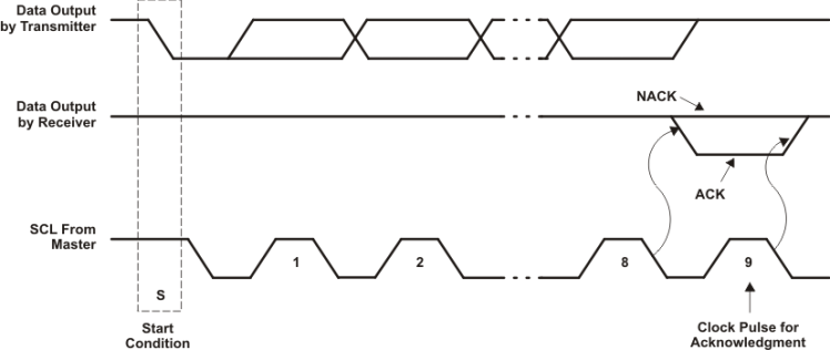
 Any number of data bytes can be transferred from the master to slave (TCA5013) between the START and STOP conditions. Each byte of eight bits is followed by one ACK bit. The master must release the SDA line before the slave can send an ACK bit. To send an ACK bit the slave pulls down the SDA line during the low phase of ACK-related clock period, so that the SDA line is stable low during the high phase of the ACK-related clock period. When the slave is addressed, it generates an ACK after each byte is received. The master is not required to generate an ACK after each byte that it receives from the slave transmitter
Figure 22 shows the timing diagram for generation of the ACK bit on the I2C interface of the TCA5013
 Figure 22. Acknowledgment on I2C Bus