JAJSFN6G September 2009 – June 2018 TCA8418
PRODUCTION DATA.
- 1 特長
- 2 アプリケーション
- 3 概要
- 4 改訂履歴
- 5 Pin Configuration and Functions
-
6 Specifications
- 6.1 Absolute Maximum Ratings
- 6.2 ESD Ratings
- 6.3 Recommended Operating Conditions
- 6.4 Thermal Information
- 6.5 Electrical Characteristics
- 6.6 I2C Interface Timing Requirements
- 6.7 Reset Timing Requirements
- 6.8 Switching Characteristics
- 6.9 Keypad Switching Characteristics
- 6.10 Typical Characteristics
- 7 Parameter Measurement Information
-
8 Detailed Description
- 8.1 Overview
- 8.2 Functional Block Diagram
- 8.3 Feature Description
- 8.4 Device Functional Modes
- 8.5 Programming
- 8.6
Register Maps
- 8.6.1 Device Address
- 8.6.2
Control Register and Command Byte
- 8.6.2.1 Configuration Register (Address 0x01)
- 8.6.2.2 Interrupt Status Register, INT_STAT (Address 0x02)
- 8.6.2.3 Key Lock and Event Counter Register, KEY_LCK_EC (Address 0x03)
- 8.6.2.4 Key Event Registers (FIFO), KEY_EVENT_A–J (Address 0x04–0x0D)
- 8.6.2.5 Keypad Lock1 to Lock2 Timer Register, KP_LCK_TIMER (Address 0x0E)
- 8.6.2.6 Unlock1 and Unlock2 Registers, UNLOCK1/2 (Address 0x0F-0x10)
- 8.6.2.7 GPIO Interrupt Status Registers, GPIO_INT_STAT1–3 (Address 0x11–0x13)
- 8.6.2.8 GPIO Data Status Registers, GPIO_DAT_STAT1–3 (Address 0x14–0x16)
- 8.6.2.9 GPIO Data Out Registers, GPIO_DAT_OUT1–3 (Address 0x17–0x19)
- 8.6.2.10 GPIO Interrupt Enable Registers, GPIO_INT_EN1–3 (Address 0x1A–0x1C)
- 8.6.2.11 Keypad or GPIO Selection Registers, KP_GPIO1–3 (Address 0x1D–0x1F)
- 8.6.2.12 GPI Event Mode Registers, GPI_EM1–3 (Address 0x20–0x22)
- 8.6.2.13 GPIO Data Direction Registers, GPIO_DIR1–3 (Address 0x23–0x25)
- 8.6.2.14 GPIO Edge/Level Detect Registers, GPIO_INT_LVL1–3 (Address 0x26–0x28)
- 8.6.2.15 Debounce Disable Registers, DEBOUNCE_DIS1–3 (Address 0x29–0x2B)
- 8.6.2.16 GPIO pull-up Disable Register, GPIO_PULL1–3 (Address 0x2C–0x2E)
- 8.6.3 CAD Interrupt Errata
- 8.6.4 Overflow Errata
- 9 Application and Implementation
- 10Power Supply Recommendations
- 11Layout
- 12デバイスおよびドキュメントのサポート
- 13メカニカル、パッケージ、および注文情報
パッケージ・オプション
メカニカル・データ(パッケージ|ピン)
- RTW|24
サーマルパッド・メカニカル・データ
- RTW|24
発注情報
10 Power Supply Recommendations
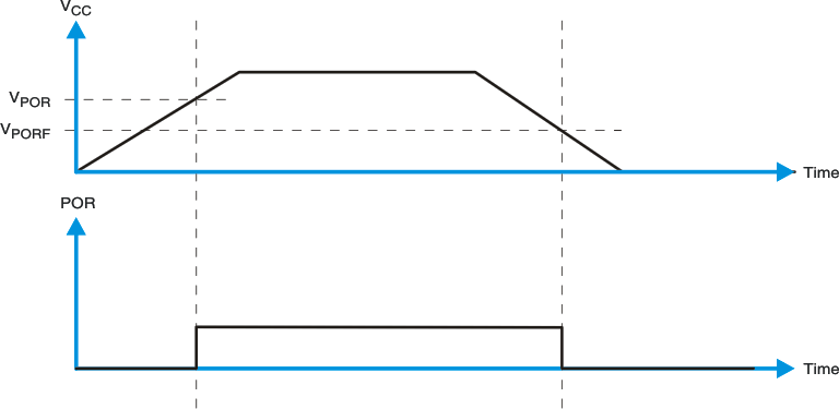
In the event of a glitch or data corruption, TCA8418 can be reset to its default conditions by using the power-on reset feature. Power-on reset requires that the device go through a power cycle to be completely reset. This reset also happens when the device is powered on for the first time in an application.
The two types of power-on reset are shown in Figure 34 and Figure 35.
 Figure 34. VCC is Lowered Below 0.2 V or 0 V and Then Ramped Up to VCC
  Figure 35. VCC is Lowered Below the POR Threshold, Then Ramped Back Up to VCC
 Table 13 specifies the performance of the power-on reset feature for TCA8418 for both types of power-on reset.
Table 13. Recommended Supply Sequencing and Ramp Rates(1)
| PARAMETER | MIN | TYP | MAX | UNIT | ||
|---|---|---|---|---|---|---|
| VCC_FT | Fall rate | See Figure 34 | 1 | 100 | ms | |
| VCC_RT | Rise rate | See Figure 34 | 0.01 | 100 | ms | |
| VCC_TRR_GND | Time to re-ramp (when VCC drops to GND) | See Figure 34 | 0.001 | ms | ||
| VCC_TRR_POR50 | Time to re-ramp (when VCC drops to VPOR_MIN – 50 mV) | See Figure 35 | 0.001 | ms | ||
| VCC_GH | Level that VCC can glitch down to, but not cause a functional disruption when VCCX_GW = 1 μs | See Figure 36 | 1.2 | V | ||
| VCC_GW | Glitch width that will not cause a functional disruption when VCCX_GH = 0.5 × VCCx | See Figure 36 | 10 | μs | ||
| VPORF | Voltage trip point of POR on falling VCC | 0.76 | 1.15 | V | ||
| VPORR | Voltage trip point of POR on rising VCC | 1.03 | 1.43 | V | ||
Glitches in the power supply can also affect the power-on reset performance of this device. The glitch width (VCC_GW) and height (VCC_GH) are dependent on each other. The bypass capacitance, source impedance, and device impedance are factors that affect power-on reset performance. Figure 36 and Table 13 provide more information on how to measure these specifications.
 Figure 36. Glitch Width and Glitch Height
 VPOR is critical to the power-on reset. VPOR is the voltage level at which the reset condition is released and all the registers and the I2C/SMBus state machine are initialized to their default states. The value of VPOR differs based on the VCC being lowered to or from 0. Figure 37 and Table 13 provide more details on this specification.
 Figure 37. VPOR
 For proper operation of the power-on reset feature, use as directed in the previous figures and table above.