JAJSGL8E December   2014  – October 2024 TCA9617B

PRODUCTION DATA  

  1.   1
  2. 特長
  3. アプリケーション
  4. 概要
  5. Pin Configuration and Functions
  6. Specifications
    1. 5.1 Absolute Maximum Ratings
    2. 5.2 ESD Ratings
    3. 5.3 Recommended Operating Conditions
    4. 5.4 Thermal Information
    5. 5.5 Electrical Characteristics
    6. 5.6 Timing Requirements
    7. 5.7 Typical Characteristics
  7.   Parameter Measurement Information
  8. Detailed Description
    1. 6.1 Overview
    2. 6.2 Functional Block Diagram
    3. 6.3 Feature Description
      1. 6.3.1 Bidirectional Level Translation
      2. 6.3.2 Low to High Transition Characteristics
      3. 6.3.3 High-to-Low Transition Characteristics
    4. 6.4 Device Functional Modes
  9. Application and Implementation
    1. 7.1 Application Information
    2. 7.2 Typical Application
      1. 7.2.1 Standard Application
        1. 7.2.1.1 Design Requirements
        2. 7.2.1.2 Detailed Design Procedure
          1. 7.2.1.2.1 Pullup Resistor Sizing
        3. 7.2.1.3 Application Curves
      2. 7.2.2 Star Application
        1. 7.2.2.1 Design Requirements
        2. 7.2.2.2 Detailed Design Procedure
        3. 7.2.2.3 Application Curves
      3. 7.2.3 Series Application
        1. 7.2.3.1 Design Requirements
        2. 7.2.3.2 Detailed Design Procedure
        3. 7.2.3.3 Application Curves
    3. 7.3 Power Supply Recommendations
    4. 7.4 Layout
      1. 7.4.1 Layout Guidelines
      2. 7.4.2 Layout Example
  10. Device and Documentation Support
    1. 8.1 ドキュメントの更新通知を受け取る方法
    2. 8.2 サポート・リソース
    3. 8.3 商標
    4. 8.4 静電気放電に関する注意事項
    5. 8.5 用語集
  11. Revision History
  12. 10Mechanical, Packaging, and Orderable Information
    1. 10.1 Tape and Reel Information

パッケージ・オプション

メカニカル・データ(パッケージ|ピン)
サーマルパッド・メカニカル・データ
発注情報

Abstract

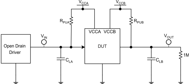
TCA9617B Test Circuit for Open-Drain Output from A to BFigure 6-1 Test Circuit for Open-Drain Output from A to B
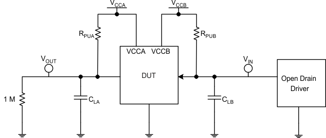
TCA9617B Test Circuit for Open-Drain Output from B to A
VCCA = 0.9V
VCCB = 2.5V
RPUA = RPUB = 240Ω on the A-side and the B-side
CLA = 200pF on A-side and CLB = 400pF on B-side (includes probe and jig capacitance)
All input pulses are supplied by generators having the following characteristics: PRR ≤ 10MHz, ZO = 50Ω, slew rate ≥ 1V/ns
The outputs are measured one at a time, with one transition per measurement.
Figure 6-2 Test Circuit for Open-Drain Output from B to A
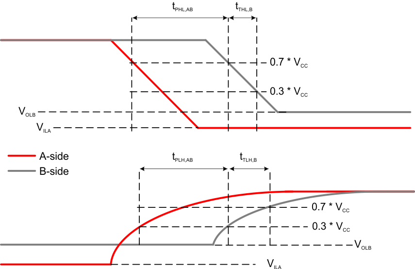
TCA9617B Propagation Delay And Transition Times (A to B)Figure 6-3 Propagation Delay And Transition Times (A to B)
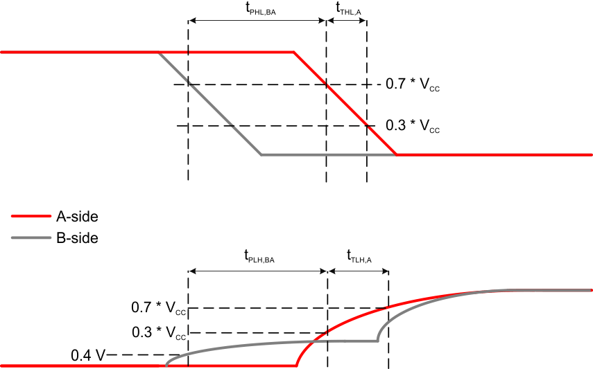
TCA9617B Propagation Delay And Transition Times (B to A)Figure 6-4 Propagation Delay And Transition Times (B to A)