JAJSKR8B October 2019 – March 2022 TCAN1144-Q1 , TCAN1145-Q1 , TCAN1146-Q1
PRODUCTION DATA
- 1 特長
- 2 アプリケーション
- 3 概要
- 4 Revision History
- 5 概要 (続き)
- 6 Device Comparison Table
- 7 Pin Configuration and Functions
- 8 Specifications
- 9 Parameter Measurement Information
-
10Detailed Description
- 10.1 Overview
- 10.2 Functional Block Diagram
- 10.3 Feature Description
- 10.4
Device Functional Modes
- 10.4.1 Normal Mode
- 10.4.2 Standby Mode
- 10.4.3 Listen Only Mode
- 10.4.4 Sleep Mode
- 10.4.5
Selective Wake-up
- 10.4.5.1 Selective Wake Mode (TCAN1145-Q1 and TCAN1146-Q1)
- 10.4.5.2 Frame Detection (TCAN1145-Q1 and TCAN1146-Q1)
- 10.4.5.3 Wake-Up Frame (WUF) Validation (TCAN1145-Q1 and TCAN1146-Q1)
- 10.4.5.4 WUF ID Validation (TCAN1145-Q1 and TCAN1146-Q1)
- 10.4.5.5 WUF DLC Validation (TCAN1145-Q1 and TCAN1146-Q1)
- 10.4.5.6 WUF Data Validation (TCAN1145-Q1 and TCAN1146-Q1)
- 10.4.5.7 Frame error counter (TCAN1145-Q1 and TCAN1146-Q1)
- 10.4.5.8 CAN FD Frame Tolerance (TCAN1145-Q1 and TCAN1146-Q1)
- 10.4.6 Fail-safe Features
- 10.4.7
Protection Features
- 10.4.7.1 Driver and Receiver Function
- 10.4.7.2 Floating Terminals
- 10.4.7.3 TXD Dominant Time Out (DTO)
- 10.4.7.4 CAN Bus Short Circuit Current Limiting
- 10.4.7.5 Thermal Shutdown
- 10.4.7.6 Under-Voltage Lockout (UVLO) and Unpowered Device
- 10.4.7.7 Watchdog (TCAN1144-Q1 and TCAN1146-Q1)
- 10.4.8 Bus Fault Detection and Communication (TCAN1144-Q1 and TCAN1146-Q1)
- 10.4.9 SPI Communication
- 10.5 Programming
- 10.6
Register Maps
- 10.6.1 DEVICE_ID_y Register (Address = 0h + formula) [reset = value]
- 10.6.2 REV_ID_MAJOR Register (Address = 8h) [reset = 01h]
- 10.6.3 REV_ID_MINOR Register (Address = 9h) [reset = 00h]
- 10.6.4 SPI_RSVD_x Register (Address = Ah + formula) [reset = 00h]
- 10.6.5 Scratch_Pad_SPI Register (Address = Fh) [reset = 00h]
- 10.6.6 MODE_CNTRL Register (Address = 10h) [reset = 04h]
- 10.6.7 WAKE_PIN_CONFIG Register (Address = 11h) [reset = 4h]
- 10.6.8 PIN_CONFIG Register (Address = 12h) [reset = 00h]
- 10.6.9 WD_CONFIG_1 Register (Address = 13h) [reset = 15h]
- 10.6.10 WD_CONFIG_2 Register (Address = 14h) [reset = 02h]
- 10.6.11 WD_INPUT_TRIG Register (Address = 15h) [reset = 00h]
- 10.6.12 WD_RST_PULSE Register (Address = 16h) [reset = 07h]
- 10.6.13 FSM_CONFIG Register (Address = 17h) [reset = 00h]
- 10.6.14 FSM_CNTR Register (Address = 18h) [reset = 00h]
- 10.6.15 DEVICE_RST Register (Address = 19h) [reset = 00h]
- 10.6.16 DEVICE_CONFIG1 Register (Address = 1Ah) [reset = 00h]
- 10.6.17 DEVICE_CONFIG2 Register (Address = 1Bh) [reset = 0h]
- 10.6.18 SWE_DIS Register (Address 1Ch) [reset = 04h]
- 10.6.19 SDO_CONFIG Register (Address = 29h) [reset = 00h]
- 10.6.20 WD_QA_CONFIG Register (Address = 2Dh) [reset = 00h]
- 10.6.21 WD_QA_ANSWER Register (Address = 2Eh) [reset = 00h]
- 10.6.22 WD_QA_QUESTION Register (Address = 2Fh) [reset = 00h]
- 10.6.23 SW_ID1 Register (Address = 30h) [reset = 00h]
- 10.6.24 SW_ID2 Register (Address = 31h) [reset = 00h]
- 10.6.25 SW_ID3 Register (Address = 32h) [reset = 00h]
- 10.6.26 SW_ID4 Register (Address = 33h) [reset = 00h]
- 10.6.27 SW_ID_MASK1 Register (Address = 34h) [reset = 00h]
- 10.6.28 SW_ID_MASK2 Register (Address = 35h) [reset = 00h]
- 10.6.29 SW_ID_MASK3 Register (Address = 36h) [reset = 00h]
- 10.6.30 SW_ID_MASK4 Register (Address = 37h) [reset = 00h]
- 10.6.31 SW_ID_MASK_DLC Register (Address = 38h) [reset = 00h]
- 10.6.32 DATA_y Register (Address = 39h + formula) [reset = 00h]
- 10.6.33 SW_RSVD_y Register (Address = 41h + formula) [reset = 00h]
- 10.6.34 SW_CONFIG_1 Register (Address = 44h) [reset = 50h]
- 10.6.35 SW_CONFIG_2 Register (Address = 45h) [reset = 00h]
- 10.6.36 SW_CONFIG_3 Register (Address = 46h) [reset = 1Fh]
- 10.6.37 SW_CONFIG_4 Register (Address = 47h) [reset = 00h]
- 10.6.38 SW_CONFIG_RSVD_y Register (Address = 48h + formula) [reset = 00h]
- 10.6.39 INT_GLOBAL Register (Address = 50h) [reset = 00h]
- 10.6.40 INT_1 Register (Address = 51h) [reset = 00h]
- 10.6.41 INT_2 Register (Address = 52h) [reset = 40h]
- 10.6.42 INT_3 Register (Address 53h) [reset = 00h]
- 10.6.43 INT_CANBUS Register (Address = 54h) [reset = 00h]
- 10.6.44 INT_GLOBAL_ENABLE (Address = 55h) [reset = 00h]
- 10.6.45 INT_ENABLE_1 Register (Address = 56h) [reset = FFh]
- 10.6.46 INT_ENABLE_2 Register (Address = 57h) [reset = 1Fh]
- 10.6.47 INT_ENABLE_3 Register (Address = 58h) [reset = 0h]
- 10.6.48 INT_ENABLE_CANBUS Register (Address = 59h) [reset = 7Fh]
- 10.6.49 INT_RSVD_y Register (Address = 5Ah + formula) [reset = 00h]
- 11Application Information Disclaimer
- 12Power Supply Recommendations
- 13Layout
- 14Device and Documentation Support
- 15Mechanical, Packaging, and Orderable Information
パッケージ・オプション
メカニカル・データ(パッケージ|ピン)
サーマルパッド・メカニカル・データ
- DMT|14
発注情報
10.4 Device Functional Modes
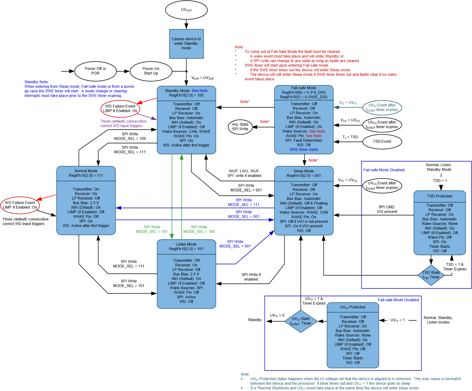
The TCAN114x-Q1 has several operating modes: normal, standby, listen, sleep and fail-safe mode and two protected modes. The first four mode selections are made by the SPI register, 8h10[2:0]. Fail-safe mode if enabled is entered due to various fault conditions. The protected modes are a modified standby modes used to protect the device or bus when fail-safe mode is disabled. The TCAN114x-Q1 automatically goes from sleep to standby mode when receiving a WUP or LWU event. When selective wake is enabled, TCAN1145-Q1 and TCAN1146-Q1, the device looks for a wake-up frame (WUF) after receiving a WUP. If a WUF is not received the device transitions back to sleep mode. See Table 10-1 for the various modes and what parts of the device are active during each mode.
The TCAN114x-Q1 state diagram figure, see Figure 10-8, Figure 10-9 and Figure 10-10 which show the biasing of the CAN bus in each of the modes of operation.
| Block | Normal | Standby | Listen | Sleep | Fail-safe | UVIO Protected | TSD Protected (Fail-safe Disabled) |
|---|---|---|---|---|---|---|---|
| nINT (If Enabled) | On | On | On | Off | Fault Determines | Off | On |
| INH | On | On | On | Off | On | On | On |
| LIMP (If Enabled): TCAN1144-Q1 TCAN1146-Q1 | Off unless WD fail | Off | Off | Off | On if Enabled | Off | Off |
| WAKE | Off | On | Off | On | See Note | Off | Off |
| SPI | On | On | On | On if VIO present | Fault Determines | Off | On |
| Watchdog: TCAN1144-Q1 TCAN1146-Q1 | On | On | Off | Off | Off | Off | Off |
| Low Power CAN RX | Off | On | Off | On | On | On | On |
| CAN Transmitter | On | Off | Off | Off | Off | Off | Off |
| CAN Receiver | On | Off | On | Off | Off | Off | Off |
Fail-safe mode has several blocks that state Fault Determines. The following provides an explanation.
- nINT and SPI can be active if the fault condition is UVCC or TSD. These blocks are off if the fault condition is UVIO.
- INH (default) in fail-safe mode is on, so the processor has power and can read which fault has occurred. When using the fail-safe counter after programmed number of wake up and go back to fail-safe cycles INH can be programmed to turn off and then on.
- The low power CAN (WUP) receiver is powered off of VSUP. A UVSUP event will cause this receiver to be off.
- Once the fail-safe counter limit has been reached and if register 8’h17[6:4] = 100b, FS_CNTR_ACT, the device will enter sleep mode and not respond to wake request. A hard reset (power cycle) is required to bring the device back to normal operation.
- In fail-safe mode the SWE timer starts and wake events are ignored until the
fault is cleared. Once fault is cleared the WAKE pin
is active.
- If the SWE timer times out the device will enter Sleep mode. This can happen even if faults are cleared and if no wake event has taken place or the device hasn't had SPI communication like changing modes.
 Figure 10-8 TCAN1145-Q1 Device State
Diagram
 Figure 10-9 TCAN1146-Q1 Device State
Diagram
 Figure 10-10 TCAN1144-Q1 Device State
Diagram
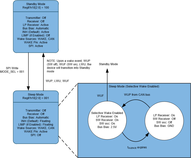
 Figure 10-11 TCAN1145-Q1 and TCAN1146-Q1 Selective Wake Enabled Sleep Mode
For the state diagrams by default SPI is off in sleep mode. If VIO is present SPI will work in sleep mode but at a reduced data rate, which would include selective wake sub state as shown in Figure 10-11.