JAJSND9A May   2021  – November 2021 TCAN11623-Q1 , TCAN11625-Q1

PRODUCTION DATA  

  1. 特長
  2. アプリケーション
  3. 概要
  4. Revision History
  5. 概要 (続き)
  6. Pin Configurations and Functions (TCAN11625)
  7. Pin Configurations and Functions (TCAN11623)
  8. Specifications
    1. 8.1 Absolute Maximum Ratings
    2. 8.2 ESD Ratings
    3. 8.3 ESD Ratings IEC Specification
    4. 8.4 Recomended Operating Conditions
    5. 8.5 Thermal Information
    6. 8.6 Power Supply Characteristics
    7. 8.7 Electrical Characteristics
    8. 8.8 Switching Characteristics
    9. 8.9 Typical Characteristics
  9. Parameter Measurement Information
  10. 10Detailed Description
    1. 10.1 Overview
    2. 10.2 Functional Block Diagram
    3. 10.3 Feature Description
      1. 10.3.1  VSUP Pin
      2. 10.3.2  VCCOUT Pin
      3. 10.3.3  VFLT Pin
      4. 10.3.4  VLDO3 Pin
      5. 10.3.5  Digital Inputs and Outputs
        1. 10.3.5.1 TXD Pin
        2. 10.3.5.2 RXD Pin
        3. 10.3.5.3 TS Pin
      6. 10.3.6  Digital Control and Timing
      7. 10.3.7  VIO Pin
      8. 10.3.8  GND
      9. 10.3.9  INH Pin
      10. 10.3.10 WAKE Pin
      11. 10.3.11 nRST Pin
      12. 10.3.12 CAN Bus Pins
      13. 10.3.13 Local Faults
        1. 10.3.13.1 TXD Dominant Timeout (TXD DTO)
        2. 10.3.13.2 Thermal Shutdown (TSD)
        3. 10.3.13.3 Under/Over Voltage Lockout
        4. 10.3.13.4 Unpowered Devices
        5. 10.3.13.5 Floating Terminals
        6. 10.3.13.6 CAN Bus Short Circuit Current Limiting
        7. 10.3.13.7 Sleep Wake Error Timer
    4. 10.4 Device Functional Modes
      1. 10.4.1 Operating Mode Description
        1. 10.4.1.1 Normal Mode
        2. 10.4.1.2 Standby Mode
        3. 10.4.1.3 Sleep Mode
          1. 10.4.1.3.1 Remote Wake Request via Wake-Up Pattern (WUP)
          2. 10.4.1.3.2 Local Wake-Up (LWU) via WAKE Input Terminal
        4. 10.4.1.4 Reset Mode
        5. 10.4.1.5 Fail-safe Mode
      2. 10.4.2 CAN Transceiver
        1. 10.4.2.1 CAN Transceiver Operation
        2. 10.4.2.2 CAN Transceiver Modes
          1. 10.4.2.2.1 CAN Off Mode
          2. 10.4.2.2.2 CAN Autonomous: Inactive and Active
          3. 10.4.2.2.3 CAN Active
        3. 10.4.2.3 Driver and Receiver Function Tables
        4. 10.4.2.4 CAN Bus States
  11. 11Application Information
    1. 11.1 Application Information Disclaimer
    2. 11.2 Typical Application
      1. 11.2.1 Design Requirements
        1. 11.2.1.1 Bus Loading, Length and Number of Nodes
      2. 11.2.2 Detailed Design Procedures
        1. 11.2.2.1 CAN Termination
    3. 11.3 Application Curves
  12. 12Power Supply Requirements
  13. 13Layout
    1. 13.1 Layout Guidelines
    2. 13.2 Layout Example
  14. 14Device and Documentation Support
    1. 14.1 Documentation Support
      1. 14.1.1 Related Documentation
    2. 14.2 Receiving Notification of Documentation Updates
    3. 14.3 サポート・リソース
    4. 14.4 Trademarks
    5. 14.5 Electrostatic Discharge Caution
    6. 14.6 Glossary
  15. 15Mechanical, Packaging, and Orderable Information

パッケージ・オプション

メカニカル・データ(パッケージ|ピン)
サーマルパッド・メカニカル・データ
発注情報

TXD Dominant Timeout (TXD DTO)

While the CAN driver is in active mode a TXD DTO circuit prevents the local node from blocking network communication in event of a hardware or software failure where TXD is held dominant longer than the time out period tTXD_DTO. The TXD DTO circuit is triggered by a falling edge on TXD. If no rising edge is seen before the time out constant of the circuit, tTXD_DTO, expires the CAN driver is disabled releasing the bus lines to the recessive level. This keeps the bus free for communication between other nodes on the network. The CAN driver is re-activated on the next dominant to recessive transition on the TXD terminal, thus clearing the dominant time out. The high-speed receiver and RXD terminal will reflect what is on the CAN bus during a TXD DTO fault. The TS terminal in driven low during a TXD DTO fault.
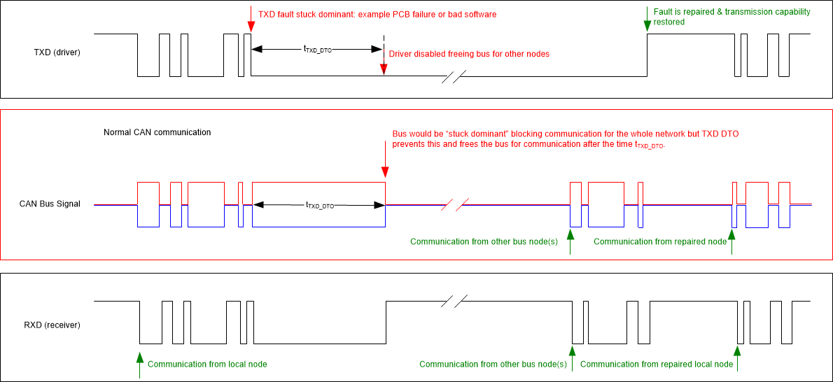
GUID-E30FD5B4-ABA8-4236-A6D4-891B4E2508AC-low.gifFigure 10-4 Timing Diagram for TXD DTO

The minimum dominant TXD time allowed by the TXD DTO circuit limits the minimum possible transmitted data rate of the device. The CAN protocol allows a maximum of eleven successive dominant bits (on TXD) for the worst case, where five successive dominant bits are followed immediately by an error frame. The minimum transmitted data rate may be calculated using the minimum tTXD_DTO time and the maximum number of successive dominant bits (11 bits).

Equation 1. Minimum Data Rate = 11 bits / tTXD_DTO = 11 bits / 1.2 ms = 9.2 kbps