JAJSOY9C March 2020 – December 2022 TCAN1463-Q1
PRODUCTION DATA
- 1 特長
- 2 アプリケーション
- 3 概要
- 4 Revision History
- 5 概要 (続き)
- 6 Pin Configuration and Functions
-
7 Specifications
- 7.1 Absolute Maximum Ratings
- 7.2 ESD Ratings
- 7.3 ESD Ratings - IEC Specifications
- 7.4 Recommended Operating Conditions
- 7.5 Thermal Information
- 7.6 Power Dissipation Ratings
- 7.7 Power Supply Characteristics
- 7.8 Electrical Characteristics
- 7.9 Timing Requirements
- 7.10 Switching Characteristics
- 7.11 Typical Characteristics
- 8 Parameter Measurement Information
-
9 Detailed Description
- 9.1 Overview
- 9.2 Functional Block Diagram
- 9.3
Feature Description
- 9.3.1 Supply Pins
- 9.3.2 Digital Inputs and Outputs
- 9.3.3 GND
- 9.3.4 INH Pin
- 9.3.5 WAKE Pin
- 9.3.6 CAN Bus Pins
- 9.3.7
Faults
- 9.3.7.1
Internal and External Fault Indicators
- 9.3.7.1.1 Power-Up (PWRON Flag)
- 9.3.7.1.2 Wake-Up Request (WAKERQ Flag)
- 9.3.7.1.3 Undervoltage Faults
- 9.3.7.1.4 CAN Bus Fault (CBF Flag)
- 9.3.7.1.5 TXD Clamped Low (TXDCLP Flag)
- 9.3.7.1.6 TXD Dominant State Timeout (TXDDTO Flag)
- 9.3.7.1.7 TXD Shorted to RXD Fault (TXDRXD Flag)
- 9.3.7.1.8 CAN Bus Dominant Fault (CANDOM Flag)
- 9.3.7.1
Internal and External Fault Indicators
- 9.3.8 Local Faults
- 9.4 Device Functional Modes
- 10Application Information Disclaimer
- 11Device and Documentation Support
- 12Mechanical, Packaging, and Orderable Information
パッケージ・オプション
メカニカル・データ(パッケージ|ピン)
サーマルパッド・メカニカル・データ
- DMT|14
発注情報
9.4.1.5.2 Local Wake-Up (LWU) via WAKE Input Terminal
The WAKE terminal is a bi-directional high-voltage reverse-battery protected input which can be used for local wake-up (LWU) requests via a voltage transition. A LWU event is triggered on either a low-to-high or high-to-low transition since it has bi-directional input thresholds. The WAKE pin could be used with a switch to VSUP or to ground. If the terminal is unused it should be pulled to VSUP or ground to avoid unwanted parasitic wake-up events.
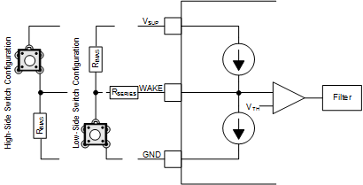
 Figure 9-9 WAKE Circuit Example
Figure 9-9 shows two possible configurations for the WAKE pin, a low-side and high-side switch configuration. The objective of the series resistor, RSERIES, is to protect the WAKE input of the device from over current conditions that may occur in the event of a ground shift or ground loss. The minimum value of RSERIES can be calculated using the maximum supply voltage, VSUPMAX, and the maximum allowable current of the WAKE pin, IIO(WAKE). RSERIES is calculated using:
With absolute maximum voltage, VSUPMAX, of 45 V and maximum allowable IIO(WAKE) of 3 mA, the minimum required RSERIES value is 15 kΩ.
The RBIAS resistor is used to set the static voltage level of the WAKE input when the switch is released. When the switch is in use in a high-side switch configuration, the RBIAS resistor in combination with the RSERIES resistor sets the WAKE pin voltage above the VIH threshold. The maximum value of RBIAS can be calculated using the maximum supply voltage, VSUPMAX, the maximum WAKE threshold voltage VIH, the maximum WAKE input current IIH and the series resistor value RSERIES. RBIAS is calculated using:
With VSUPMAX of 45 V, VIH of 44 V at IIH of 3 µA, the RBIAS resistor value must be less than 330 kΩ. It is recommended to use RSeries less than 50 kΩ to provide better margin for the WAKE pin voltage to rise above VIH when the switch is released.
The LWU circuitry is active in sleep mode.
The WAKE circuitry is switched off in normal mode.