SPRSPB4A June 2024 – December 2024 TDA4APE-Q1 , TDA4VPE-Q1
PRODUCTION DATA
- 1
- 1 Features
- 2 Applications
- 3 Description
- 4 Device Comparison
-
5 Terminal Configuration and Functions
- 5.1 Pin Diagrams
- 5.2 Pin Attributes
- 5.3
Signal Descriptions
- 13
- 5.3.1 ADC
- 5.3.2 CPSW2G
- 5.3.3 CPTS
- 5.3.4 CSI
- 5.3.5 DDRSS
- 5.3.6 Display Port
- 5.3.7 DMTIMER
- 5.3.8 DSI
- 5.3.9 DSS
- 5.3.10 ECAP
- 5.3.11 EPWM
- 5.3.12 EQEP
- 5.3.13 GPIO
- 5.3.14 GPMC
- 5.3.15 HYPERBUS
- 5.3.16 I2C
- 5.3.17 I3C
- 5.3.18 MCAN
- 5.3.19 MCASP
- 5.3.20 MCSPI
- 5.3.21 MDIO
- 5.3.22 MMC
- 5.3.23 OSPI
- 5.3.24 PCIE
- 5.3.25 SERDES
- 5.3.26 SGMII
- 5.3.27 UART
- 5.3.28 UFS
- 5.3.29 USB
- 5.3.30 Emulation and Debug
- 5.3.31 System and Miscellaneous
- 5.3.32 Power
- 5.4 Pin Connectivity Requirements
-
6 Specifications
- 6.1 Absolute Maximum Ratings
- 6.2 ESD Ratings
- 6.3 Power-On-Hour (POH) Limits
- 6.4 Recommended Operating Conditions
- 6.5 Operating Performance Points
- 6.6
Electrical Characteristics
- 6.6.1 I2C, Open-Drain, Fail-Safe (I2C OD FS) Electrical Characteristics
- 6.6.2 Fail-Safe Reset (FS Reset) Electrical Characteristics
- 6.6.3 HFOSC/LFOSC Electrical Characteristics
- 6.6.4 eMMCPHY Electrical Characteristics
- 6.6.5 SDIO Electrical Characteristics
- 6.6.6 CSI2/DSI D-PHY Electrical Characteristics
- 6.6.7 ADC12B Electrical Characteristics
- 6.6.8 LVCMOS Electrical Characteristics
- 6.6.9 USB2PHY Electrical Characteristics
- 6.6.10 SerDes 2-L-PHY/4-L-PHY Electrical Characteristics
- 6.6.11 UFS M-PHY Electrical Characteristics
- 6.6.12 eDP/DP AUX-PHY Electrical Characteristics
- 6.6.13 DDR0 Electrical Characteristics
- 6.7 VPP Specifications for One-Time Programmable (OTP) eFuses
- 6.8 Thermal Resistance Characteristics
- 6.9 Temperature Sensor Characteristics
- 6.10
Timing and Switching Characteristics
- 6.10.1 Timing Parameters and Information
- 6.10.2
Power Supply Sequencing
- 6.10.2.1 Power Supply Slew Rate Requirement
- 6.10.2.2 Combined MCU and Main Domains Power- Up Sequencing
- 6.10.2.3 Combined MCU and Main Domains Power- Down Sequencing
- 6.10.2.4 Isolated MCU and Main Domains Power- Up Sequencing
- 6.10.2.5 Isolated MCU and Main Domains Power- Down Sequencing
- 6.10.2.6 Independent MCU and Main Domains, Entry and Exit of MCU Only Sequencing
- 6.10.2.7 Independent MCU and Main Domains, Entry and Exit of DDR Retention State
- 6.10.2.8 Independent MCU and Main Domains, Entry and Exit of GPIO Retention Sequencing
- 6.10.3 System Timing
- 6.10.4
Clock Specifications
- 6.10.4.1 Input and Output Clocks / Oscillators
- 6.10.4.2 Output Clocks
- 6.10.4.3 PLLs
- 6.10.4.4 Module and Peripheral Clocks Frequencies
- 6.10.5
Peripherals
- 6.10.5.1 ATL
- 6.10.5.2
CPSW2G
- 6.10.5.2.1 CPSW2G MDIO Interface Timings
- 6.10.5.2.2 CPSW2G RMII Timings
- 6.10.5.2.3
CPSW2G RGMII Timings
- 6.10.5.2.3.1 RGMII[x]_RXC Timing Requirements – RGMII Mode
- 6.10.5.2.3.2 CPSW2G Timing Requirements for RGMII[x]_RD[3:0], and RGMII[x]_RCTL – RGMII Mode
- 6.10.5.2.3.3 CPSW2G RGMII[x]_TXC Switching Characteristics – RGMII Mode
- 6.10.5.2.3.4 RGMII[x]_TD[3:0], and RGMII[x]_TX_CTL Switching Characteristics – RGMII Mode
- 6.10.5.3 CSI-2
- 6.10.5.4 DDRSS
- 6.10.5.5 DSS
- 6.10.5.6 eCAP
- 6.10.5.7 EPWM
- 6.10.5.8 eQEP
- 6.10.5.9 GPIO
- 6.10.5.10 GPMC
- 6.10.5.11 HyperBus
- 6.10.5.12 I2C
- 6.10.5.13 I3C
- 6.10.5.14 MCAN
- 6.10.5.15 MCASP
- 6.10.5.16 MCSPI
- 6.10.5.17 MMCSD
- 6.10.5.18 CPTS
- 6.10.5.19 OSPI
- 6.10.5.20 OLDI
- 6.10.5.21 PCIE
- 6.10.5.22 Timers
- 6.10.5.23 UART
- 6.10.5.24 USB
- 6.10.6 Emulation and Debug
-
7 Applications,
Implementation, and Layout
- 7.1 Device Connection and Layout Fundamentals
- 7.2 Peripheral- and Interface-Specific Design Information
- 8 Device and Documentation Support
- 9 Revision History
- 10Mechanical, Packaging, and Orderable Information
パッケージ・オプション
デバイスごとのパッケージ図は、PDF版データシートをご参照ください。
メカニカル・データ(パッケージ|ピン)
- AND|1063
サーマルパッド・メカニカル・データ
発注情報
6.10.4.1.1.2 Shunt Capacitance
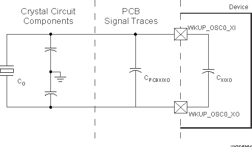
The crystal circuit must also be designed such that it does not exceed the maximum shunt capacitance for WKUP_OSC0 operating conditions defined in Table 6-21. Shunt capacitance, Cshunt, of the crystal circuit is a combination of crystal shunt capacitance and parasitic contributions. PCB signal traces which connect crystal circuit components to WKUP_OSC0 have mutual parasitic capacitance to each other, CPCBXIXO, where the PCB designer should be able to extract mutual parasitic capacitance between these signal traces. The device package also has mutual parasitic capacitance, CXIXO, where this mutual parasitic capacitance value is defined in Table 6-22.
PCB routing should be designed to minimize mutual capacitance between XI and XO signal traces. This is typically done by keeping signal traces short and not routing them in close proximity. Mutual capacitance can also be minimized by placing a ground trace between these signals when the layout requires them to be routed in close proximity. It is important to minimize the mutual capacitance on the PCB to provide as much margin as possible when selecting a crystal.
 Figure 6-26 Shunt Capacitance
A crystal should be chosen such that the below equation is satisfied. CO in the equation is the maximum shunt capacitance specified by the crystal manufacturer.
Cshunt ≥ CO + CPCBXIXO + CXIXO
For example, the equation would be satisfied when the crystal being used is 25 MHz with an ESR = 30 Ω, CPCBXIXO = 0.04 pF, CXIXO = 0.01 pF, and shunt capacitance of the crystal is less than or equal to 6.95 pF.