JAJSOC1H March 2000 – March 2022 TFP401 , TFP401A
PRODUCTION DATA
- 1 特長
- 2 アプリケーション
- 3 概要
- 4 Revision History
- 5 概要 (続き)
- 6 Pin Configuration and Functions
- 7 Specifications
- 8 Parameter Measurement Information
- 9 Detailed Description
- 10Applications and Implementation
- 11Power Supply Recommendations
- 12Layout
- 13Device and Documentation Support
- 14Mechanical, Packaging, and Orderable Information
パッケージ・オプション
メカニカル・データ(パッケージ|ピン)
- PZP|100
サーマルパッド・メカニカル・データ
- PZP|100
発注情報
8 Parameter Measurement Information
 Figure 8-1 Rise and
Fall Times of Data and Control Signals
 Figure 8-2 Rise
and Fall Times of ODCK
 Figure 8-3 ODCK
Frequency
 Figure 8-4 Data
Setup and Hold Times to Rising and Falling Edges of ODCK
Figure 8-4 Data
Setup and Hold Times to Rising and Falling Edges of ODCK![ODCK
High to QE[23:0] Staggered Data Output GUID-DA37585F-0460-4604-982E-05A97D64DFE3-low.gif](/ods/images/JAJSOC1H/GUID-DA37585F-0460-4604-982E-05A97D64DFE3-low.gif) Figure 8-5 ODCK
High to QE[23:0] Staggered Data Output
Figure 8-5 ODCK
High to QE[23:0] Staggered Data Output Figure 8-7 Delay
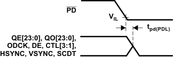
From PD Low to Hi-Z Outputs
 Figure 8-9 Delay
From PD Low to High Before Inputs Are Active
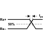
 Figure 8-6 Analog Input Intra-Pair Differential Skew
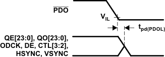
 Figure 8-8 Delay
From PDO Low to Hi-Z Outputs
 Figure 8-10 Minimum Time PD Low
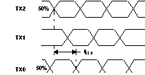
 Figure 8-11 Analog
Input Channel-to-Channel Skew
 Figure 8-12 Time
Between DE Transitions to SCDT Low and SCDT High
 Figure 8-13 Minimum
DE Low and Maximum DE High