SLOS217I July 1998 – December 2024 THS3001
PRODUCTION DATA
- 1
- 1 Features
- 2 Applications
- 3 Description
- 4 Pin Configuration and Functions
- 5 Specifications
- 6 Detailed Description
- 7 Application and Implementation
- 8 Device and Documentation Support
- 9 Revision History
- 10Mechanical, Packaging, and Orderable Information
パッケージ・オプション
デバイスごとのパッケージ図は、PDF版データシートをご参照ください。
メカニカル・データ(パッケージ|ピン)
- D|8
- DGN|8
サーマルパッド・メカニカル・データ
- DGN|8
発注情報
7.1.2 Noise Calculations
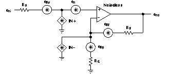
Noise can cause errors on small signals. This problem is especially true for amplifying small signals coming over a transmission line or an antenna. The noise model for current-feedback (CFB) amplifiers is the same as for voltage-feedback (VFB) amplifiers. The only difference between CFB and VFB amplifiers is that CFB amplifiers generally specify different current-noise parameters for each input, whereas VFB amplifiers usually only specify one noise-current parameter. Figure 7-1 shows the noise model. This model includes all of the noise sources as follows:
- en = Amplifier internal voltage noise (nV/√Hz)
- IN+ = Noninverting current noise (pA/√Hz)
- IN– = Inverting current noise (pA/√Hz)
- eRx = Thermal voltage noise associated with each resistor (eRx = 4 kTRx)
 Figure 7-1 Noise Model
The total equivalent input noise density (eni) is calculated by using the following equation:

To get the equivalent output noise of the amplifier, just multiply the equivalent input noise density (eni) by the overall amplifier gain (AV).

The previous equations show that to keep noise at a minimum, use small-value resistors. As the closed-loop gain is increased (by reducing RG), the input noise is reduced considerably because of the parallel resistance term. This result leads to the general conclusion that the most dominant noise sources are the source resistor (RS) and the internal amplifier noise voltage (en). Noise is summed in a root-mean-squares method; therefore, noise sources smaller than 25% of the largest noise source can be effectively ignored. This threshold can greatly simplify the formula and make noise calculations much easier.