SBOS766B February 2016 – February 2016 THS3217
PRODUCTION DATA.
- 1 Features
- 2 Applications
- 3 Description
- 4 Revision History
- 5 Device Comparison Table
- 6 Pin Configuration and Functions
-
7 Specifications
- 7.1 Absolute Maximum Ratings
- 7.2 ESD Ratings
- 7.3 Recommended Operating Conditions
- 7.4 Thermal Information
- 7.5 Electrical Characteristics: D2S
- 7.6 Electrical Characteristics: OPS
- 7.7 Electrical Characteristics: D2S + OPS
- 7.8 Electrical Characteristics: Midscale (DC) Reference Buffer
- 7.9 Typical Characteristics: D2S + OPS
- 7.10 Typical Characteristics: D2S Only
- 7.11 Typical Characteristics: OPS only
- 7.12 Typical Characteristics: Midscale (DC) Reference Buffer
- 7.13 Typical Characteristics: Switching Performance
- 7.14 Typical Characteristics: Miscellaneous Performance
- 8 Parameter Measurement Information
-
9 Detailed Description
- 9.1 Overview
- 9.2 Functional Block Diagram
- 9.3 Feature Description
- 9.4 Device Functional Modes
-
10Application and Implementation
- 10.1
Application Information
- 10.1.1
Typical Applications
- 10.1.1.1 High-Frequency, High-Voltage, Dual-Output Line Driver for AWGs
- 10.1.1.2 High-Voltage Pulse-Generator
- 10.1.1.3 Single-Supply, AC-Coupled, Piezo Element Driver
- 10.1.1.4 Output Common-Mode Control Using the Midscale Buffer as a Level Shifter
- 10.1.1.5 Differential I/O Driver With independent Common-Mode Control
- 10.1.1
Typical Applications
- 10.1
Application Information
- 11Power Supply Recommendations
- 12Layout
- 13Device and Documentation Support
- 14Mechanical, Packaging, and Orderable Information
7 Specifications
7.1 Absolute Maximum Ratings
over operating free-air temperature range (unless otherwise noted)(1)| MIN | MAX | UNIT | ||
|---|---|---|---|---|
| Voltage | Supply, +VCC – (–VCC) | 16.2 | V | |
| Input/output | (–VCC) – 0.5 | (+VCC) + 0.5 | ||
| Differential input voltage (IN+ – IN–) | ±8 | |||
| Current | Continuous input current (IN+, IN–, VMID_IN, VIN+, VIN–)(2) | ±10 | mA | |
| Continuous output current(2) | ±30 | |||
| Temperature | Operating, TA | –55 | 105 | °C |
| Junction, TJ | –45 | 150 | ||
| Storage, Tstg | –65 | 150 | ||
(1) Stresses beyond those listed under Absolute Maximum Ratings may cause permanent damage to the device. These are stress ratings only, which do not imply functional operation of the device at these or any other conditions beyond those indicated under Recommended Operating Conditions. Exposure to absolute-maximum-rated conditions for extended periods may affect device reliability.
(2) Long-term continuous current for electromigration limits.
7.2 ESD Ratings
| VALUE | UNIT | |||
|---|---|---|---|---|
| V(ESD) | Electrostatic discharge | Human-body model (HBM), per ANSI/ESDA/JEDEC JS-001(1) | ±1500 | V |
| Charged-device model (CDM), per JEDEC specification JESD22-C101(2) | ±1000 | |||
(1) JEDEC document JEP155 states that 500-V HBM allows safe manufacturing with a standard ESD control process.
(2) JEDEC document JEP157 states that 250-V CDM allows safe manufacturing with a standard ESD control process.
7.3 Recommended Operating Conditions
over operating free-air temperature range (unless otherwise noted)| MIN | NOM | MAX | UNIT | ||
|---|---|---|---|---|---|
| +VCC | Positive supply voltage | 4 | 6 | 7.9 | V |
| –VCC | Negative supply voltage | –4 | –6 | –7.9 | V |
| TA | Operating free-air temperature | –40 | 25 | 85 | °C |
7.4 Thermal Information
| THERMAL METRIC(1) | THS3217 | UNIT | |
|---|---|---|---|
| RGV (VQFN) | |||
| 16 PINS | |||
| RθJA | Junction-to-ambient thermal resistance | 45 | °C/W |
| RθJC(top) | Junction-to-case (top) thermal resistance | 45 | °C/W |
| RθJB | Junction-to-board thermal resistance | 22 | °C/W |
| ψJT | Junction-to-top characterization parameter | 1 | °C/W |
| ψJB | Junction-to-board characterization parameter | 22 | °C/W |
| RθJC(bot) | Junction-to-case (bottom) thermal resistance | 4 | °C/W |
(1) Thermal impedance reported with backside thermal pad soldered to heat spreading plane. For more information about traditional and new thermal metrics, see the Semiconductor and IC Package Thermal Metrics application report, SPRA953.
7.5 Electrical Characteristics: D2S
at +VCC = 6.0 V, –VCC = –6.0 V, AV = 2 V/V, 25-Ω source impedance, input common-mode voltage (VIC) = 0.25 V, external OPS input selected (PATHSEL ≥ 1.3 V), VREF = GND, RLOAD = 100 Ω, and TJ ≈ 25˚C (unless otherwise noted)| PARAMETER | TEST CONDITIONS | MIN | TYP | MAX | UNIT | TEST LEVEL (1) | |
|---|---|---|---|---|---|---|---|
| AC PERFORMANCE (Power Stage Disabled: DISABLE pin ≥ 1.3 V) (5) | |||||||
| Small-signal bandwidth (SSBW) | VOUT = 250 mVPP, peaking < 1.0 dB | 800 | MHz | C | |||
| Large-signal bandwidth (LSBW) | VOUT = 2 VPP | 500 | MHz | C | |||
| Bandwidth for 0.2-dB flatness | VOUT = 2 VPP | 250 | MHz | C | |||
| Slew rate(2) | VOUT = 4-V step | 2500 | V/µs | C | |||
| Over- and undershoot | Input tr = 1 ns, VOUT = 2-V step | 6% | C | ||||
| Rise and fall time | Input tr = 1 ns, VOUT = 2-V step | 1.2 | ns | C | |||
| Settling time to 0.1% | Input tr = 1 ns, VOUT = 2-V step | 5 | ns | C | |||
| 2nd-order harmonic distortion (HD2) | f = 20 MHz, VOUT= 2 VPP | –68 | dBc | C | |||
| 3rd-order harmonic distortion (HD3) | f = 20 MHz, VOUT= 2 VPP | –86 | dBc | C | |||
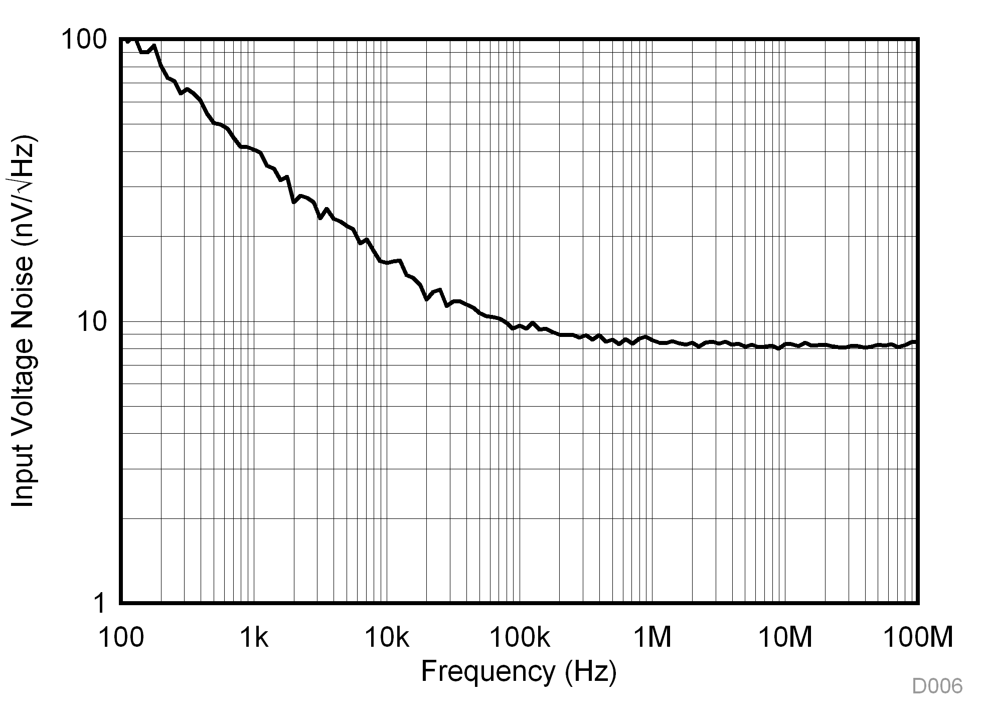
| Output voltage noise | f > 200 kHz | 18 | nV/√Hz | C | |||
| Input current noise (each input) | f > 200 kHz | 2.0 | pA/√Hz | C | |||
| Output impedance | f = 20 MHz | 0.8 | Ω | C | |||
| DC PERFORMANCE (5) | |||||||
| Differential to single-ended gain | ±100-mV output | 1.975 | 2.0 | 2.025 | V/V | A | |
| Differential to single-ended gain drift | TJ = –40°C to +125°C | –20 | –24 | ppm/°C | B | ||
| VREF input pin gain | Differential inputs = 0 V, VREF = ±100 mV |
0.985 | 1.0 | 1.015 | V/V | A | |
| VREF input pin gain drift | TJ = –40°C to +125°C | –70 | –95 | ppm/°C | B | ||
| Output offset voltage | TJ = 25°C | –35 | ±8 | 35 | mV | A | |
| TJ = 0°C to 70°C | –43 | 40 | mV | B | |||
| TJ = –40°C to +125°C | –54 | 47 | mV | B | |||
| Output offset voltage drift | TJ = –40°C to +125°C | -40 | –115 | –190 | µV/°C | B | |
| Input bias current – each input(3) | TJ = 25°C | –4 | ±2 | 4 | µA | A | |
| TJ = 0°C to 70°C | –4.2 | 4.2 | µA | B | |||
| TJ = –40°C to +125°C | –4.3 | 4.5 | µA | B | |||
| Input bias current drift | TJ = –40°C to +125°C | 1 | 3 | 5 | nA/°C | B | |
| Input offset current | TJ = 25°C | –400 | ±50 | 400 | nA | A | |
| TJ = 0°C to 70°C | –700 | 940 | nA | B | |||
| TJ = –40°C to +125°C | –1180 | 1600 | nA | B | |||
| Input offset current drift | TJ = –40°C to +125°C | –12 | ±1 | 12 | nA/°C | B | |
| INPUTS(4) | |||||||
| Common-mode input negative supply headroom | TJ = 25°C | 1.8 | 1.9 | V | A | ||
| TJ = –40°C to +85°C | 2.0 | V | B | ||||
| Common-mode input positive supply headroom | TJ = 25°C | 1.3 | 1.4 | V | A | ||
| TJ = –40°C to +125°C | 1.5 | V | B | ||||
| Common-mode rejection ratio (CMRR) | –1 V ≤ VIC ≤ 3 V | 47 | 55 | dB | A | ||
| Input impedance differential mode | VCM = 0 V | 50 || 2.4 | kΩ || pF | C | |||
| Input impedance common mode | VCM = 0 V | 90 || 2.4 | kΩ || pF | C | |||
| OUTPUT(6) | |||||||
| Output voltage headroom to either supply | TJ = 25°C | 1.1 | 1.35 | 1.55 | V | A | |
| TJ = –40°C to +125°C | V | B | |||||
| Output current drive | TJ = 25°C, ±1.16 VPP, RLOAD = 20 Ω | 50 | 70 | mA | A | ||
| DC Output Impedance | Load current = ±20 mA | 0.2 | 0.45 | Ω | A | ||
| POWER SUPPLY (D2S Stage + Midsupply Buffer Only; Output Power Stage Disabled: DISABLE pin ≥ 1.3 V) | |||||||
| Bipolar-supply operating range | ±4.0 | ±6.0 | ±7.9 | V | A | ||
| Single-supply operating range | 8 | 12 | 15.8 | V | B | ||
| Supply current | ±6-V supplies | 31 | 34 | 36 | mA | A | |
| Supply current temperature coefficient | 7 | µA/°C | C | ||||
(1) Test levels (all values set by characterization and simulation): (A) 100% tested at TA≈ TJ≈ 25°C; over temperature limits by characterization and simulation. (B) Not tested in production; limits set by characterization and simulation. (C) Typical value only for information. DC limits tested with no self-heating. Add internal self heating to TA for TJ.
(2) This slew rate is the average of the rising and falling time estimated from the large-signal bandwidth as: (Vpeak / √2) × 2π × f–3dB.
(3) Currents out of pin treated as a positive polarity.
(4) Applies to input pins 2 (IN+) and 3 (IN–).
(5) Output measured at pin 6.
(6) Output measured at pin 6.
7.6 Electrical Characteristics: OPS
at +VCC = 6.0 V, –VCC = –6.0 V, 25-Ω D2S source impedance, D2S input common-mode voltage (VIC) = 0.25 V, VREF = GND, RF = 249 Ω(1), RG = 162 Ω, AV = 2.5 V/V, OPS RLOAD = 100 Ω, OPS enabled (DISABLE ≤ 0.7 V or floated), external OPS input selected (PATHSEL ≥ 1.3 V), and TJ ≈ 25˚C (unless otherwise noted)| PARAMETER | TEST CONDITIONS | MIN | TYP | MAX | UNIT | TEST LEVEL (2) | |
|---|---|---|---|---|---|---|---|
| AC PERFORMANCE (4) | |||||||
| Small-signal bandwidth (SSBW) | VOUT = 100 mVPP, peaking < 1.0 dB | 950 | MHz | C | |||
| Large-signal bandwidth (LSBW) | VOUT = 5 VPP | 500 | MHz | C | |||
| Bandwidth for 0.2-dB flatness | VOUT = 5 VPP | 110 | MHz | C | |||
| Slew rate(3) | VOUT = 5-V step | 5500 | V/µs | C | |||
| Over- and undershoot | Input tr = 1 ns, VOUT = 5-V step | 8% | C | ||||
| Rise and fall time | Input tr = 1 ns, VOUT = 5-V step | 1.1 | ns | C | |||
| Settling time to 0.1% | Input tr = 1 ns, VOUT = 5-V step | 5 | ns | C | |||
| 2nd-order harmonic distortion (HD2) | f = 20 MHz, VOUT= 5 VPP | –69 | dBc | C | |||
| 3rd-order harmonic distortion (HD3) | f = 20 MHz, VOUT= 5 VPP | –73 | dBc | C | |||
| Noninverting input voltage noise | f > 200 kHz | 3.2 | nV/√Hz | C | |||
| Noninverting input current noise | f > 200 kHz | 2.8 | pA/√Hz | C | |||
| Inverting input current noise | f > 200 kHz | 30 | pA/√Hz | C | |||
| Closed-loop ac output impedance | f = 20 MHz | 0.40 | Ω | C | |||
| DC PERFORMANCE (4) | |||||||
| Open-loop transimpedance gain(1) | VOUT = ±1 V, RLOAD= 500-Ω | 600 | 1200 | kΩ | A | ||
| Closed-loop gain | 0.1% external RF and RG resistors | 2.495 | 2.515 | 2.53 | V/V | A | |
| INPUT | |||||||
| External input offset voltage (pin 9 to pin12) | TJ = 25°C | –12 | ±2.5 | 12 | mV | A | |
| TJ = 0°C to 70°C | –20 | 17 | mV | B | |||
| TJ = –40°C to +125°C | –31 | 24 | mV | B | |||
| External input offset voltage drift (pin 9 to pin12) | TJ = –40°C to +125°C | -45 | –115 | –190 | µV/°C | B | |
| Internal input offset voltage (pin 6 to pin 12) | TJ = 25°C | –12 | ±2.5 | 12 | mV | A | |
| TJ = 0°C to 70°C | –23 | 18 | mV | B | |||
| TJ = –40°C to +125°C | –35 | 27 | mV | B | |||
| Internal input offset voltage drift (pin 6 to pin 12) | TJ = –40°C to +125°C | –70 | –150 | –235 | µV/°C | B | |
| External to internal input offset voltage match | TJ = 25°C | ±1.2 | mV | C | |||
| External noninverting input bias current (pin 9)(5) | TJ = 25°C | –5 | ±5 | 15 | µA | A | |
| TJ = 0°C to 70°C | –5.2 | 15.4 | µA | B | |||
| TJ = –40°C to +125°C | –5.6 | 15.9 | µA | B | |||
| External noninverting input bias current drift (pin 9) | TJ = –40°C to +125°C | –3 | 3 | 9 | nA/°C | B | |
| Inverting input bias current – either input selected(5) | TJ = 25°C | –40 | ±5 | 40 | µA | A | |
| TJ = 0°C to 70°C | –51 | 46 | µA | B | |||
| TJ = –40°C to +125°C | –65 | 56 | µA | B | |||
| Inverting input bias current drift | TJ = –40°C to +125°C | –250 | –120 | –10 | nA/°C | B | |
| Input headroom to either supply | TJ = 25°C | 2.6 | 3.0 | V | A | ||
| Common-mode rejection ratio (CMRR) | 47 | 49 | dB | A | |||
| Noninverting input resistance | 17.6 | 18.5 | 22.4 | kΩ | A | ||
| Noninverting input capacitance | 3.3 | pF | C | ||||
| Open-loop inverting input impedance | 42 | Ω | C | ||||
| OUTPUT(6) | |||||||
| Output voltage headroom to either supply | RLOAD = 500 Ω | 1.1 | 1.3 | 1.4 | V | A | |
| Linear output current | TJ = 25°C, ±2.5 V into 26-Ω RLOAD | 95 | 120 | mA | A | ||
| Peak output current | 0-V output, RLOAD < 0.2 Ω | 135 | 170 | mA | A | ||
| DC output impedance | 0-V output, load current = ±40 mA | 0.05 | 0.10 | Ω | A | ||
| Internal RF | 17.6 | 18.5 | 22.4 | kΩ | A | ||
| PATHSEL (Pin 4; Logic Reference = Pin 7 = GND) | |||||||
| Input low logic level | Internal path selected | 0.7 | 0.9 | V | A | ||
| Input high logic level | External input selected at VIN (pin 9) | 0.9 | 1.3 | V | A | ||
| Input voltage range | –0.5 | +VCC | V | A | |||
| PATHSEL voltage when floated | Internal input from D2S selected | 0 | 20 | 40 | mV | A | |
| Input pin bias current(7) | 0-V input | 0 | 4 | µA | A | ||
| 3.3-V input | –150 | –250 | µA | A | |||
| Input pin impedance | 18 || 1.5 | kΩ || pF | C | ||||
| Switching time | To 1% of final value | 80 | ns | C | |||
| Input switching glitch | Both inputs at GND | 50 | mV | C | |||
| Deselected input dc isolation | ± 2-V input | 70 | 80 | dB | A | ||
| Deselected input ac isolation | 2 VPP, at 20-MHz input | 55 | 65 | dB | C | ||
| DISABLE (Pin 10; Logic Reference = Pin 7 = GND) | |||||||
| Input low logic level | 0.7 | 0.9 | V | A | |||
| Input high logic level | 0.9 | 1.3 | V | A | |||
| Shutdown control voltage range | –0.5 | +VCC | V | B | |||
| Shutdown voltage when floated | Output stage enabled | 0 | 20 | 40 | mV | A | |
| Input pin bias current(7) | 0-V input | 0 | 4 | µA | A | ||
| 3.3-V input | –150 | –250 | µA | A | |||
| Input pin impedance | 18 || 1.5 | kΩ || pF | C | ||||
| Switching time (turn on or off) | To 10% of final value | 200 | ns | C | |||
| Shutdown dc isolation (either input) | ±2-V input | 70 | 80 | dB | A | ||
| Shutdown ac isolation (either input) | 2 VPP at 20-MHz input | 55 | 65 | dB | C | ||
| POWER SUPPLY | |||||||
| Bipolar-supply operating range | ±4.0 | ±6.0 | ±7.9 | V | A | ||
| Single-supply operating range | 8 | 12 | 15.8 | V | B | ||
| Supply current (OPS only) | ±6-V supplies | 18.5 | 21 | 24.5 | mA | A | |
| Disabled supply current in OPS | ±6-V supplies | 2.0 | 2.4 | 3.0 | mA | C | |
| Logic reference current at pin 7(7) | Pins 4, 7, and 10 held at 0 V | 200 | 280 | 380 | µA | A | |
(1) Output power stage includes an internal 18.5-kΩ feedback resistor. This internal resistor, in parallel with an external 249-Ω RF and 162-Ω RG, results in a gain of 2.5 V/V after including a nominal gain loss of 0.9935 V/V due to the input buffer and loop-gain effects.
(2) Test levels (all values set by characterization and simulation): (A) 100% tested at TA≈ TJ≈ 25°C; over temperature limits by characterization and simulation. (B) Not tested in production; limits set by characterization and simulation. (C) Typical value only for information. DC limits tested with no self-heating. Add internal self heating to TA for TJ.
(3) This slew rate is the average of the rising and falling time estimated from the large-signal bandwidth as: (Vpeak / √2) × 2π × f–3dB.
(4) Output measured at pin 11.
(5) Currents out of pin treated as a positive polarity.
(6) Output measured at pin 11.
(7) Currents out of pin treated as a positive polarity.
7.7 Electrical Characteristics: D2S + OPS
at +VCC = 6.0 V, –VCC = –6.0 V, 25-Ω D2S source impedance, D2S input VIC = 0.25 V, Internal path selected to OPS (PATHSEL ≤ 0.7 V or floated), VREF = GND, combined AV = 5 V/V, D2S RLOAD= 200 Ω, RF = 249 Ω(1), RG = 162 Ω (OPS AV = 2.5 V/V), OPS enabled (DISABLE ≤ 0.7 V or floated), OPS RLOAD = 100 Ω, and TJ ≈ 25˚C (unless otherwise noted)| PARAMETER | TEST CONDITIONS | MIN | TYP | MAX | UNIT | TEST LEVEL (2) | |
|---|---|---|---|---|---|---|---|
| AC PERFORMANCE(4) | |||||||
| Small-signal bandwidth (SSBW) | VOUT = 100 mVPP, peaking < 1.5 dB | 800 | MHz | C | |||
| Large-signal bandwidth (LSBW) | VOUT = 5 VPP | 500 | MHz | C | |||
| Bandwidth for 0.2-dB flatness | VOUT = 2 VPP | 100 | MHz | C | |||
| Slew rate(3) | VOUT = 8-V step | 5000 | V/µs | C | |||
| Over- and undershoot | Input tr = 1 ns, VOUT = 5-V step | 8% | C | ||||
| Rise and fall time | Input tr = 1 ns, VOUT = 5-V step | 1.1 | ns | C | |||
| Settling time to 0.1% | Input tr = 1 ns, VOUT = 5-V step | 7 | ns | C | |||
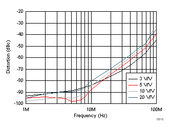
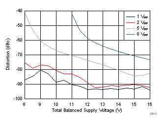
| 2nd-order harmonic distortion (HD2) | f = 20 MHz, VOUT= 5 VPP | –60 | dBc | C | |||
| 3rd-order harmonic distortion (HD3) | f = 20 MHz, VOUT= 5 VPP | –75 | dBc | C | |||
| Output voltage noise | f > 200 kHz | 45 | nV/√Hz | C | |||
| DC PERFORMANCE(4) | |||||||
| Total gain D2S to OPS output(1) | 0.1% tolerance, dc, ±100-mV output test | 4.92 | 5.02 | 5.12 | V/V | A | |
| POWER SUPPLY (Combined D2S, OPS, and Midscale Reference Buffer) | |||||||
| Bipolar-supply operating range | ±4.0 | ±6.0 | ±7.9 | V | A | ||
| Single-supply operating range | 8 | 12 | 15.8 | V | B | ||
| Supply current | ±6-V supplies | 51 | 54 | 57 | mA | A | |
| Supply current temperature coefficient | 10 | µA/°C | C | ||||
(1) Output power stage includes an internal 18.5-kΩ feedback resistor. This internal resistor, in parallel with an external 249-Ω RF and 162-Ω RG, results in a gain of 2.5 V/V after including a nominal gain loss of 0.9935 V/V due to the input buffer and loop-gain effects.
(2) Test levels (all values set by characterization and simulation): (A) 100% tested at TA≈ TJ≈ 25°C; over temperature limits by characterization and simulation. (B) Not tested in production; limits set by characterization and simulation. (C) Typical value only for information.
(3) This slew rate is the average of the rising and falling time estimated from the large-signal bandwidth as: (Vpeak / √2) × 2π × f–3dB.
(4) Output measured at pin 11.
7.8 Electrical Characteristics: Midscale (DC) Reference Buffer
at +VCC = 6.0 V, –VCC = –6.0 V, RLOAD = 150 Ω at pin 15, and TJ ≈ 25˚C (unless otherwise noted)| PARAMETER | TEST CONDITIONS | MIN | TYP | MAX | UNIT | TEST LEVEL (1) | |
|---|---|---|---|---|---|---|---|
| AC PERFORMANCE (Output measured at pin 15) | |||||||
| Small-signal bandwidth (SSBW) | VOUT = 100 mVPP | 400 | MHz | C | |||
| Large-signal bandwidth (LSBW) | VOUT = 1 VPP | 110 | MHz | C | |||
| Slew rate(2) | VOUT = 4-V step | 250 | V/µs | C | |||
| Input voltage noise | f > 200 kHz | 4.4 | nV/√Hz | C | |||
| Input current noise | f > 200 kHz | 2.3 | pA/√Hz | C | |||
| AC output impedance | f = 20 MHz | 1.0 | Ω | C | |||
| DC AND I/O PERFORMANCE (RS = 25 Ω, and output measured at pin 15, unless otherwise noted) | |||||||
| Buffer gain | VI = ±1 V, RLOAD = 200 Ω | .9985 | 0.999 | 1.001 | V/V | A | |
| Buffer gain drift | TJ = –40°C to +125°C | –1.5 | –2.0 | ppm/°C | B | ||
| Output offset from midsupply | Input floating, pin 1 open | –120 | 30 | 70 | mV | A | |
| Output offset voltage | TJ = 25°C, input driven to 0 V from 0-Ω source | –1.0 | 4.0 | 15 | mV | A | |
| Input offset voltage drift | TJ = –40°C to +125°C, input driven to 0 V | –4 | 3 | 10 | µV/°C | B | |
| Input bias current(3) | TJ = 25°C | –15 | ±1 | 15 | µA | A | |
| Input bias current drift | TJ = –40°C to +125°C | –8 | –2 | 3 | nA/°C | B | |
| Input/output headroom to either supply | TJ = 25°C, gain change < 1% | 1.1 | 1.4 | V | A | ||
| Input impedance | Internal 50-kΩ divider resistors to each supply | 22 || 1.5 | kΩ || pF | C | |||
| Linear output current into resistive load | ±2.25 V into 36 Ω | 40 | 65 | mA | A | ||
| DC output impedance | Load current = ±30 mA | 0.21 | Ω | C | |||
(1) Test levels (all values set by characterization and simulation): (A) 100% tested at TA≈ TJ≈ 25°C; over temperature limits by characterization and simulation. (B) Not tested in production; limits set by characterization and simulation. (C) Typical value only for information.
(2) This slew rate is the average of the rising and falling time estimated from the large-signal bandwidth as: (VPEAK / √2) × 2π × f–3dB.
(3) Currents out of pin treated as a positive polarity.
7.9 Typical Characteristics: D2S + OPS
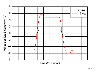
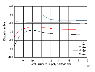
at +VCC = 6 V, –VCC = –6 V, 25-Ω D2S source impedance , VIC = 0.25 V, Internal path selected (PATHSEL = GND), VREF = GND, D2S RLOAD = 200 Ω at pin 6, RF = 249 Ω, RG = 162 Ω, OPS AV = 2.5 V/V, OPS On (DISABLE = GND), and OPS RLOAD = 100 Ω at pin 11 (unless otherwise noted)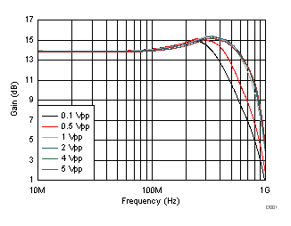
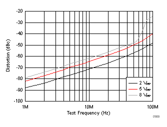
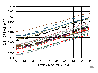
| 26 units shown |
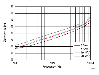
| VOUT = 5 VPP |
| Test frequency = 20 MHz |
| 25-Ω source impedance on each D2S input |
| VOUT = 5 VPP |
| Test frequency = 20 MHz |
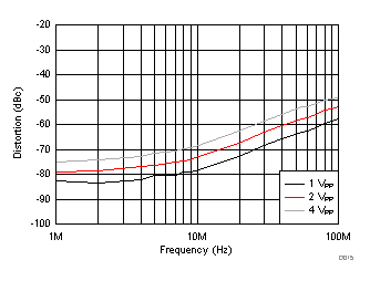
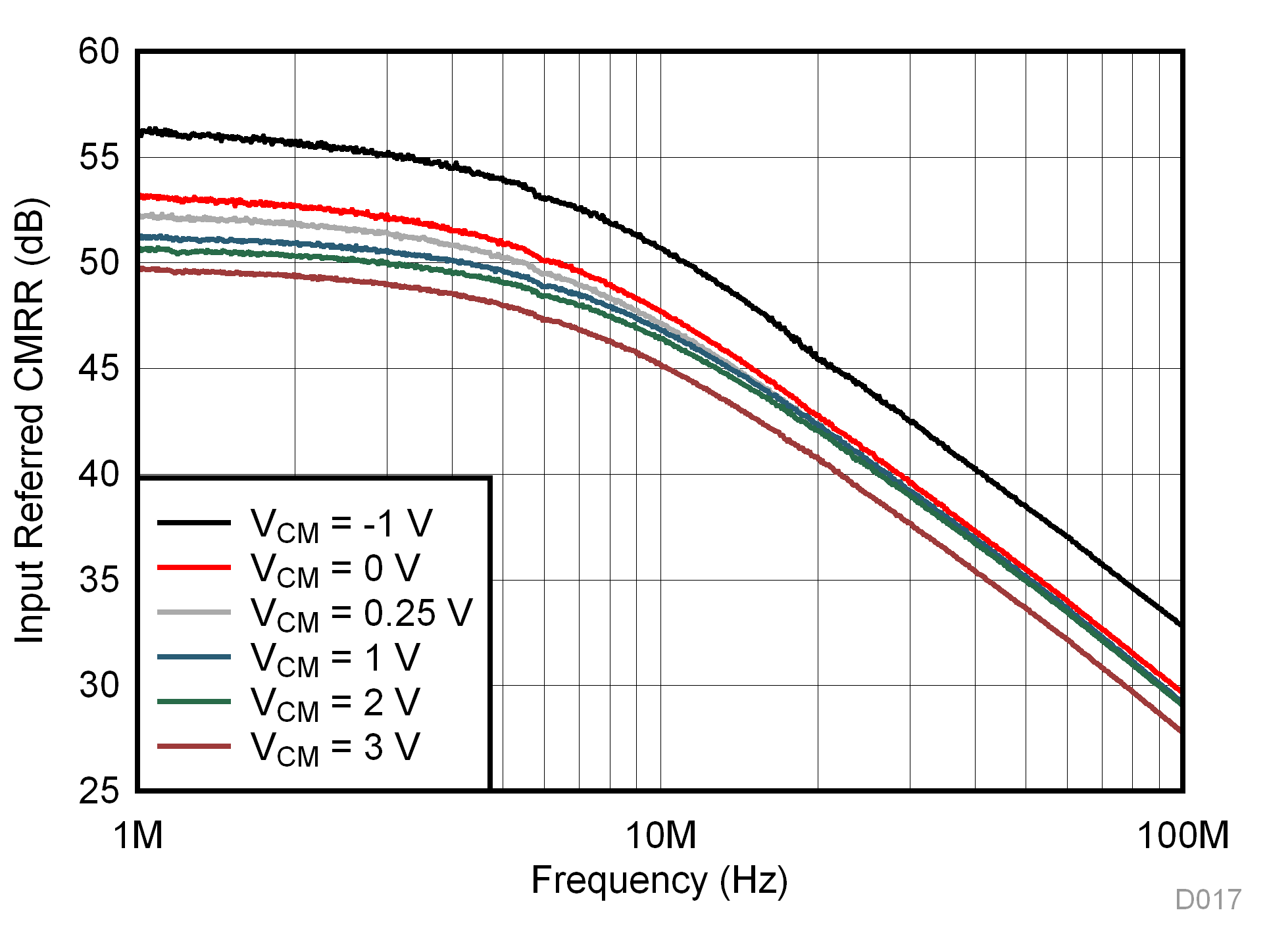
7.10 Typical Characteristics: D2S Only
at +VCC = 6.0 V, –VCC = –6.0 V, fixed gain of 2 V/V, 25-Ω D2S source impedance, VIC = 0.25 V, external path selected (PATHSEL = +VCC), VREF = GND, and D2S RLOAD = 100 Ω at pin 6 (unless otherwise noted)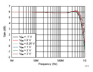
| VOUT = 250 mVPP |
| RLOAD = 200 Ω |
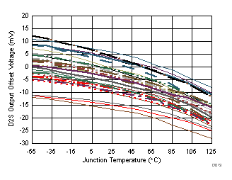
| 30 units shown |
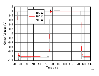
| ±1-V output pulse |
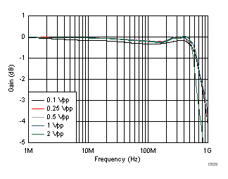
| 25-Ω D2S source impedance on each input |
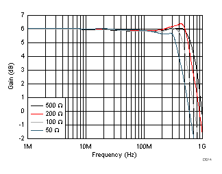
| VOUT = 2 VPP |
| RLOAD = 200 Ω |
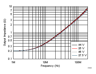
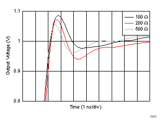
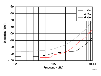
| ±1-V output pulse |
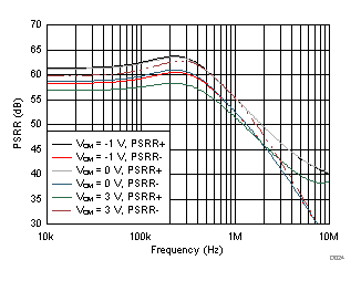
7.11 Typical Characteristics: OPS only
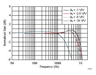
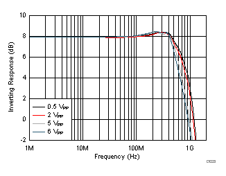
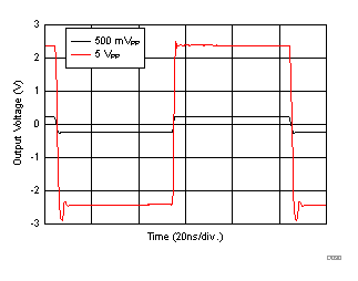
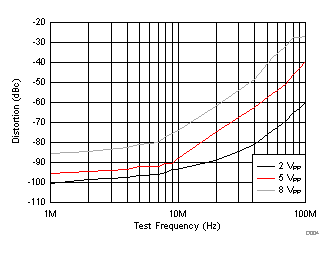
at +VCC = 6.0 V, –VCC = –6.0 V, 25-Ω D2S source impedance, VREF = GND, RF = 249 Ω, RG = 162 Ω, OPS AV = 2.5V/V, OPS RLOAD = 100 Ω at pin 11, OPS enabled (DISABLE = GND), and external input path selected (PATHSEL = +VCC) (unless otherwise noted)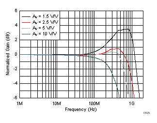
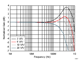
| VOUT = 100 mVPP, see Table 2 for RF values vs gain |
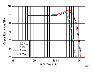
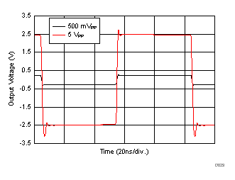
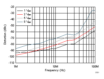
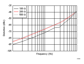
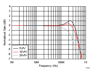
| VOUT = 5 VPP |
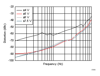
| VOUT = 5 VPP |
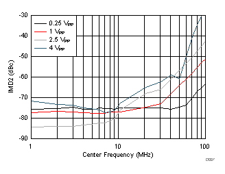
| ±100-kHz tone separation, output voltage for each tone |
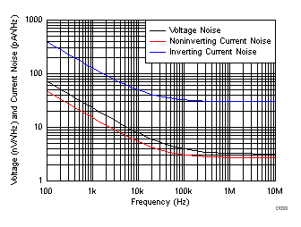
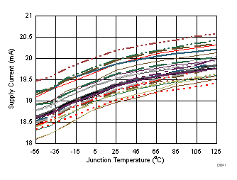
| 30 units shown |
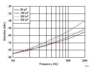
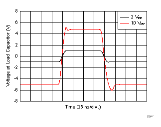
| RF = 205 Ω, AV = 5 V/V, VOUT = 10 VPP, see Figure 43 for RS value |
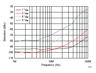
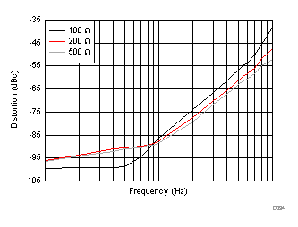
| VOUT = 5 VPP |
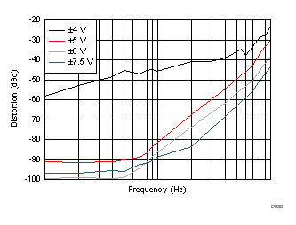
| VOUT = 5 VPP |
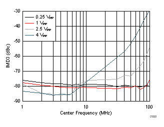
| ±100-kHz tone separation, output voltage for each tone |
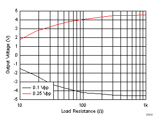
| Output swing with better than 0.1% linearity |
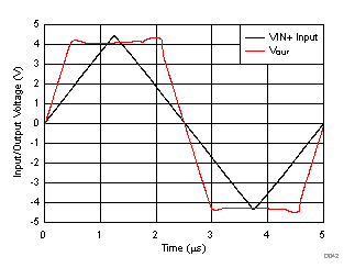
| ±4.5-V input triangular wave, OPS AV = 2.5 V/V |
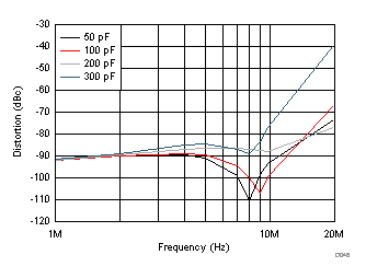
| RF = 205 Ω, AV = 5 V/V, VOUT = 10 VPP, see Figure 43 for RS value |
7.12 Typical Characteristics: Midscale (DC) Reference Buffer
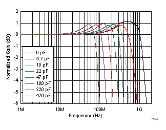
at +VCC = 6.0 V, –VCC = –6.0 V, RLOAD = 150 Ω, and TA ≈ 25˚C (unless otherwise noted)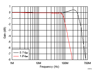
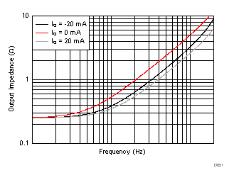
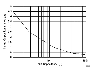
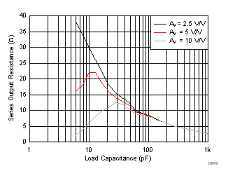
| RLOAD = 150 Ω in parallel with CLOAD, see the Midscale Buffer ROUT Versus CLOAD Measurement section for circuit setup |
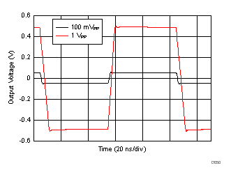
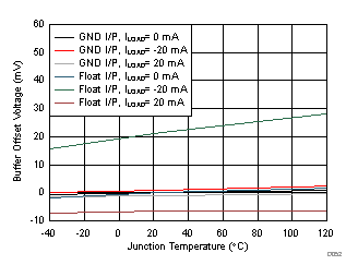
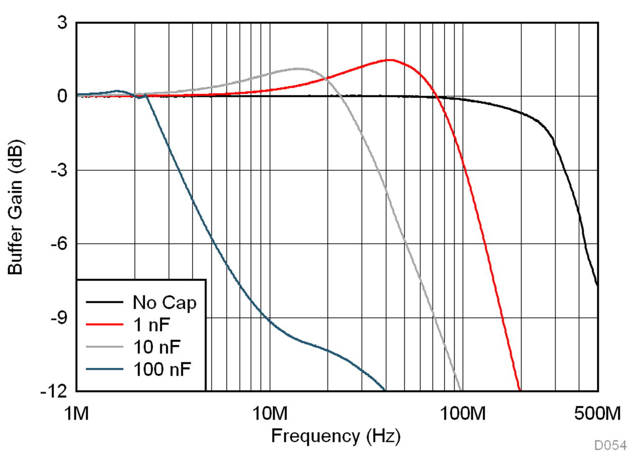
| VOUT = 100 mVPP, RLOAD = 150 Ω in parallel with CLOAD, see Midscale Buffer ROUT Versus CLOAD Measurement for circuit setup |
7.13 Typical Characteristics: Switching Performance
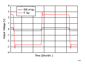
at +VCC = 6 V, –VCC = –6 V, 25-Ω D2S source impedance , VIC = 0.25 V, Internal path selected (PATHSEL = GND), VREF = GND, D2S RLOAD = 200 Ω at pin 6, RF = 249 Ω, RG = 162 Ω, OPS On (DISABLE = GND), and OPS RLOAD = 100 Ω at pin 11 (unless otherwise noted)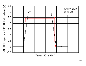
| D2S Inputs: IN+ = IN– = GND, OPS input: VIN+ = 1 V |
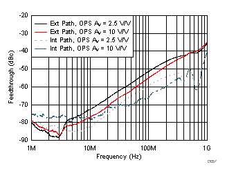
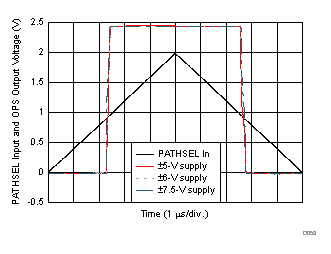
| D2S inputs: IN+ = IN– = GND, OPS input: VIN+ = 1 V |
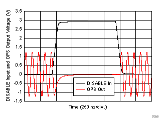
| PATHSEL = high, OPS input: VIN+ = 1 VPP , 10-MHz sine wave |
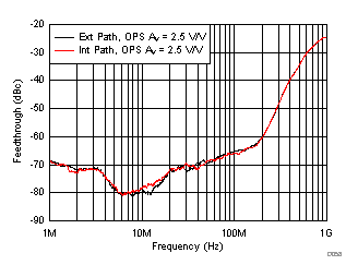
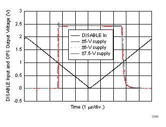
| PATHSEL = high, OPS input: VIN+ = 1 V |
7.14 Typical Characteristics: Miscellaneous Performance
at +VCC = 6 V, –VCC = –6 V, 50-Ω D2S source impedance , VIC = 0.25 V, internal path selected (PATHSEL = GND), VREF = GND, D2S RLOAD = 100 Ω at pin 6, RF = 249 Ω, RG = 162 Ω, OPS on (DISABLE = GND), and OPS RLOAD = 100 Ω at pin 11 (unless otherwise noted)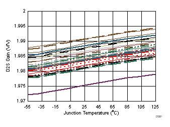
| 30 units shown |
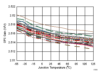
| 29 units shown |
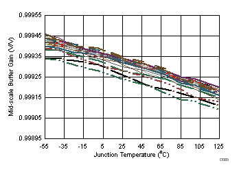
| 30 units shown |
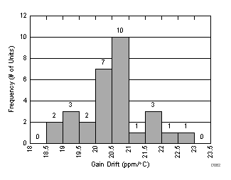
| 30 units from –40°C to +125°C |
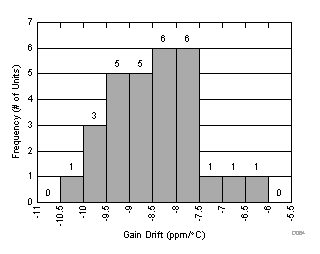
| 29 units from –40°C to +125°C |
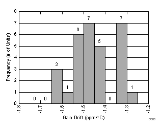
| 30 units from –40°C to +125°C |
