JAJSFG7L June 1999 – July 2024 THS4031 , THS4032
PRODUCTION DATA
- 1
- 1 特長
- 2 アプリケーション
- 3 概要
- 4 Pin Configuration and Functions
- 5 Specifications
- 6 Detailed Description
- 7 Application and Implementation
- 8 Device and Documentation Support
- 9 Revision History
- 10Mechanical, Packaging, and Orderable Information
パッケージ・オプション
デバイスごとのパッケージ図は、PDF版データシートをご参照ください。
メカニカル・データ(パッケージ|ピン)
- D|8
- DGN|8
サーマルパッド・メカニカル・データ
- DGN|8
発注情報
7.1.1 Driving a Capacitive Load
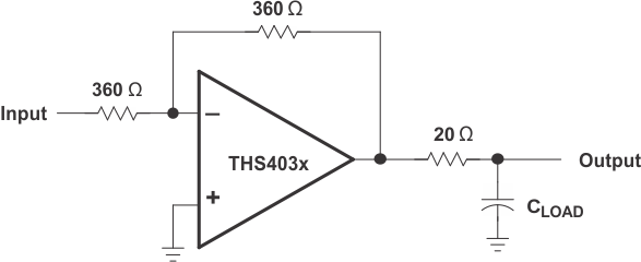
The THS403x devices are internally compensated to maximize bandwidth and slew-rate performance. Take additional precautions when driving capacitive loads with a high-performance amplifier to maintain stability. As a result of the internal compensation, significant capacitive loading directly on the output node decreases the device phase margin, and potentially leads to high-frequency ringing or oscillations. Therefore, for capacitive loads greater than 10pF, place an isolation resistor in series with the output of the amplifier. Figure 7-1 shows this configuration. For most applications, a minimum resistance of 20Ω is recommended. In 75Ω transmission systems, setting the series resistor value to 75Ω is a beneficial choice because this value isolates any capacitance loading and provides source impedance matching.
 Figure 7-1 Driving a Capacitive Load