SLOS432B April 2004 – October 2015 THS4281
PRODUCTION DATA.
- 1 Features
- 2 Applications
- 3 Description
- 4 Revision History
- 5 Pin Configuration and Functions
-
6 Specifications
- 6.1 Absolute Maximum Ratings
- 6.2 ESD Ratings
- 6.3 Recommended Operating Conditions
- 6.4 Thermal Information
- 6.5 Electrical Characteristics, VS = 3 V (VS+ = 3 V, VS- = GND)
- 6.6 Electrical Characteristics, VS = 5 V (VS+ = 5 V, VS- = GND)
- 6.7 Electrical Characteristics, VS = ±5 V
- 6.8 Dissipation Ratings
- 6.9 Typical Characteristics
- 7 Detailed Description
- 8 Application and Implementation
- 9 Power Supply Recommendations
- 10Layout
- 11Device and Documentation Support
- 12Mechanical, Packaging, and Orderable Information
パッケージ・オプション
デバイスごとのパッケージ図は、PDF版データシートをご参照ください。
メカニカル・データ(パッケージ|ピン)
- D|8
- DBV|5
- DGK|8
サーマルパッド・メカニカル・データ
発注情報
10 Layout
10.1 Layout Guidelines
Achieving optimum performance with a high-frequency amplifier like the THS4281 requires careful attention to board layout parasitics and external component types. See the EVM layout figures (Figure 76 to Figure 79) in the Design Tools section.
Recommendations that optimize performance include:
- Minimize parasitic capacitance to any ac ground for all of the signal I/O pins. Parasitic capacitance on the output and inverting input pins can cause instability and on the noninverting input, it can react with the source impedance to cause unintentional band limiting. To reduce unwanted capacitance, a window around the signal I/O pins should be opened in all of the ground and power planes around those pins. Otherwise, ground and power planes should be unbroken elsewhere on the board.
- Minimize the distance (< 0.1 inch) from the power-supply pins to high-frequency, 0.1-μF decoupling capacitors. Avoid narrow power and ground traces to minimize inductance. The power-supply connections should always be decoupled as described above.
- Careful selection and placement of external components preserves the high-frequency performance of the THS4281. Resistors should be a low reactance type. Surface-mount resistors work best and allow a tighter overall layout. Metal-film, axial-lead resistors can also provide good high-frequency performance. Again, keep the leads and PCB trace length as short as possible. Never use wire-wound type resistors in a high-frequency application. Because the output pin and inverting input pin are the most sensitive to parasitic capacitance, always position the feedback and series output resistor, if any, as close as possible to the output pin. Other network components, such as noninverting input termination resistors, should also be placed close to the package. Excessively high resistor values can create significant phase lag that can degrade performance. Keep resistor values as low as possible, consistent with load-driving considerations. It is suggested that a good starting point for design is to set the Rf to 2 kΩ for low-gain, noninverting applications. Doing this automatically keeps the resistor noise terms reasonable and minimizes the effect of parasitic capacitance.
- Connections to other wideband devices on the board should be made with short direct traces or through onboard transmission lines. For short connections, consider the trace and the input to the next device as a lumped capacitive load. Relatively wide traces (50 mils to 100 mils) should be used, preferably with ground and power planes opened up around them. Low parasitic capacitive loads (< 4 pF) may not need an R(ISO), because the THS4281 is nominally compensated to operate at unity gain (+1 V/V) with a 2-pF capacitive load. Higher capacitive loads without an R(ISO) are allowed as the signal gain increases. If a long trace is required, and the 6-dB signal loss intrinsic to a doubly terminated transmission line is acceptable, implement a matched impedance transmission line using microstrip or stripline techniques (consult an ECL design handbook for microstrip and stripline layout techniques). A matching series resistor into the trace from the output of the THS4281 is used as well as a terminating shunt resistor at the input of the destination device. Remember also that the terminating impedance is the parallel combination of the shunt resistor and the input impedance of the destination device: this total effective impedance should be set to match the trace impedance. If the 6-dB attenuation of a doubly-terminated transmission line is unacceptable, a long trace can be series-terminated at the source end only. Treat the trace as a capacitive load in this case, and use a series resistor (R(ISO) = 10 Ω to 100 Ω, as noted Driving Capacitive Loads) to isolate the capacitive load. If the input impedance of the destination device is low, there is signal attenuation due to the voltage divider formed by R(ISO) into the terminating impedance. A 50-Ω environment is normally not necessary onboard, and in fact a higher impedance environment improves distortion as shown in the distortion versus load plots.
- Socketing a high-speed part like the THS4281 is not recommended. The additional lead length and pin-to-pin capacitance introduced by the socket can create a troublesome parasitic network which can make it almost impossible to achieve a smooth, stable frequency response. Best results are obtained by soldering the THS4281 onto the board.
10.2 Layout Examples
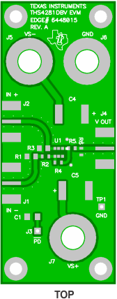 Figure 76. THS4281EVM Layout (Top Layer and Silkscreen Layer)
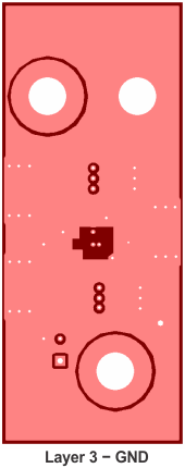 Figure 78. THS4281EVM Board Layout
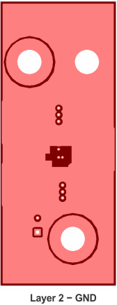 Figure 77. THS4281EVM Board Layout
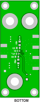 Figure 79. THS4281EVM Board Layout
10.3 Thermal Considerations
The THS4281 does not incorporate automatic thermal shutoff protection, so the designer must take care to ensure that the design does not violate the absolute maximum junction temperature of the device. Failure may result if the absolute maximum junction temperature of +150°C is exceeded. For long-term dependability, the junction temperature should not exceed +125°C.
The thermal characteristics of the device are dictated by the package and the PCB. Maximum power dissipation for a given package can be calculated using the following formula.
where
- PDmax is the maximum power dissipation in the amplifier (W).
- Tmax is the absolute maximum junciton temperature (ºC).
- TA is the ambient temperature (ºC).
- θJA = θJC + θCA
- θJC is the thermal coefficient from the silicon junctions to the case (ºC/W).
- θJA is the thermal coefficient from the case to ambient air (ºC/W).
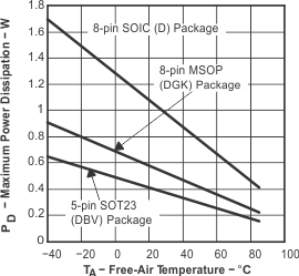
ΘJA = 180.8°C/W for 8-Pin MSOP (DGK)
ΘJA = 255.4°C/W for 5-Pin SOT−23 (DBV)
TJ = 125°C, No Airflow
When determining whether or not the device satisfies the maximum power dissipation requirement, it is important to consider not only quiescent power dissipation, but also dynamic power dissipation. Often maximum power dissipation is difficult to quantify because the signal pattern is inconsistent, but an estimate of the RMS value can provide a reasonable analysis.