SLOS823D December 2012 – March 2020 THS4531A
PRODUCTION DATA.
- 1 Features
- 2 Applications
- 3 Description
- 4 Revision History
- 5 Related Products
- 6 Pin Configuration and Functions
- 7 Specifications
- 8 Detailed Description
-
9 Application and Implementation
- 9.1
Application Information
- 9.1.1 Frequency Response, and Output Impedance
- 9.1.2 Distortion
- 9.1.3 Slew Rate, Transient Response, Settling Time, Overdrive, Output Voltage, and Turnon and Turnoff Time
- 9.1.4 Common-Mode and Power Supply Rejection
- 9.1.5 VOCM Input
- 9.1.6 Balance Error
- 9.1.7 Single-Supply Operation
- 9.1.8 Low-Power Applications and the Effects of Resistor Values on Bandwidth
- 9.1.9 Driving Capacitive Loads
- 9.1.10 Audio Performance
- 9.1.11 Audio On and Off Pop Performance
- 9.2
Typical Applications
- 9.2.1 SAR ADC Performance: THS4531A and ADS8321 Combined Performance
- 9.2.2 Audio ADC Driver Performance: THS4531A and PCM4204 Combined Performance
- 9.2.3 SAR ADC Performance: THS4531A and ADS7945 Combined Performance
- 9.2.4 Differential-Input to Differential-Output Amplifier
- 9.2.5 Single-Ended to Differential FDA Configuration
- 9.2.6 Single-Ended Input to Differential Output Amplifier
- 9.2.7 Differential Input to Single-Ended Output Amplifier
- 9.1
Application Information
- 10Power Supply Recommendations
- 11Layout
- 12Device and Documentation Support
- 13Mechanical, Packaging, and Orderable Information
9.2.5.1 Input Impedance
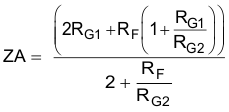
The designs so far have included a source impedance, RS, that must be matched by RT and RG1. The total impedance at the junction of RT and RG1 for the circuit of Figure 97 is the parallel combination of RT to ground, and the ZA (active impedance) presented by RG1. The expression for ZA, assuming RG2 is set to obtain the differential divider balance, is given by Equation 5:
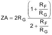
For designs that do not need impedance matching, for instance where the input is driven from the low-impedance output of another amplifier, RG1 = RG2 is the single-to-differential design used without an RT to ground. Setting RG1 = RG2 = RG in Equation 5 produces Equation 6, which is the input impedance of a simple-input FDA driven from a low-impedance, single-ended source.

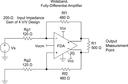
In this case, setting a target gain as RF / RG ≡ α, and then setting the desired input impedance allows the RG element to be resolved first. Then the RF is set to get the target gain. For example, targeting an input impedance of 200 Ω with a gain of 4 V/V, Equation 7 calculates the RG value. Multiplying this required RG value by a gain
of 4 gives the RF value and the design of Figure 94.

 Figure 94. 200-Ω Input Impedance, Single-Ended to Differential DC-Coupled Design With Gain of 4 V/V
 After being designed, this circuit can also be AC-coupled by adding blocking caps in series with the two 120-Ω RG resistors. This active input impedance has the advantage of increasing the apparent load to the prior stage using lower resistors values, leading to lower output noise for a given gain target.
