SLOS823D December 2012 – March 2020 THS4531A
PRODUCTION DATA.
- 1 Features
- 2 Applications
- 3 Description
- 4 Revision History
- 5 Related Products
- 6 Pin Configuration and Functions
- 7 Specifications
- 8 Detailed Description
-
9 Application and Implementation
- 9.1
Application Information
- 9.1.1 Frequency Response, and Output Impedance
- 9.1.2 Distortion
- 9.1.3 Slew Rate, Transient Response, Settling Time, Overdrive, Output Voltage, and Turnon and Turnoff Time
- 9.1.4 Common-Mode and Power Supply Rejection
- 9.1.5 VOCM Input
- 9.1.6 Balance Error
- 9.1.7 Single-Supply Operation
- 9.1.8 Low-Power Applications and the Effects of Resistor Values on Bandwidth
- 9.1.9 Driving Capacitive Loads
- 9.1.10 Audio Performance
- 9.1.11 Audio On and Off Pop Performance
- 9.2
Typical Applications
- 9.2.1 SAR ADC Performance: THS4531A and ADS8321 Combined Performance
- 9.2.2 Audio ADC Driver Performance: THS4531A and PCM4204 Combined Performance
- 9.2.3 SAR ADC Performance: THS4531A and ADS7945 Combined Performance
- 9.2.4 Differential-Input to Differential-Output Amplifier
- 9.2.5 Single-Ended to Differential FDA Configuration
- 9.2.6 Single-Ended Input to Differential Output Amplifier
- 9.2.7 Differential Input to Single-Ended Output Amplifier
- 9.1
Application Information
- 10Power Supply Recommendations
- 11Layout
- 12Device and Documentation Support
- 13Mechanical, Packaging, and Orderable Information
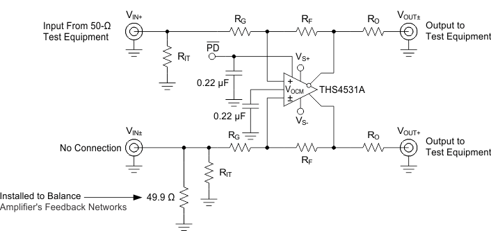
9.1.3 Slew Rate, Transient Response, Settling Time, Overdrive, Output Voltage, and Turnon and Turnoff Time
The circuit shown in Figure 71 is used to measure slew rate, transient response, settling time, overdrive recovery, and output voltage swing. Turnon and turnoff times are measured with 50-Ω input termination on the PD input, by replacing the 0.22-µF capacitor with 49.9-Ω resistor.
 Figure 71. Slew Rate, Transient Response, Settling Time, ZO, Overdrive Recovery, VOUT Swing, and Turn-On and Turn-Off Test Circuit