JAJSI65C November 2015 – October 2024 THS4541-Q1
PRODUCTION DATA
- 1
- 1 特長
- 2 アプリケーション
- 3 概要
- 4 Device Comparison Table
- 5 Pin Configuration and Functions
-
6 Specifications
- 6.1 Absolute Maximum Ratings
- 6.2 ESD Ratings
- 6.3 Recommended Operating Conditions
- 6.4 Thermal Information
- 6.5 Electrical Characteristics: (Vs+) – Vs– = 5 V
- 6.6 Electrical Characteristics: (Vs+) – Vs– = 3 V
- 6.7 Typical Characteristics: 5-V Single Supply
- 6.8 Typical Characteristics: 3-V Single Supply
- 6.9 Typical Characteristics: 3-V to 5-V Supply Range
-
7 Parameter Measurement Information
- 7.1 Example Characterization Circuits
- 7.2 Frequency-Response Shape Factors
- 7.3 I/O Headroom Considerations
- 7.4 Output DC Error and Drift Calculations and the Effect of Resistor Imbalances
- 7.5 Noise Analysis
- 7.6 Factors Influencing Harmonic Distortion
- 7.7 Driving Capacitive Loads
- 7.8 Thermal Analysis
-
8 Detailed Description
- 8.1 Overview
- 8.2 Functional Block Diagram
- 8.3 Feature Description
- 8.4
Device Functional Modes
- 8.4.1
Operation from Single-Ended Sources to Differential Outputs
- 8.4.1.1 AC-Coupled Signal Path Considerations for Single-Ended Input to Differential Output Conversion
- 8.4.1.2 DC-Coupled Input Signal Path Considerations for Single-Ended to Differential Conversion
- 8.4.1.3 Resistor Design Equations for the Single-Ended to Differential Configuration of the FDA
- 8.4.1.4 Input Impedance for the Single-Ended to Differential FDA Configuration
- 8.4.2 Differential-Input to Differential-Output Operation
- 8.4.1
Operation from Single-Ended Sources to Differential Outputs
- 9 Application and Implementation
- 10Device and Documentation Support
- 11Revision History
- 12Mechanical, Packaging, and Orderable Information
パッケージ・オプション
メカニカル・データ(パッケージ|ピン)
- RGT|16
サーマルパッド・メカニカル・データ
- RGT|16
発注情報
8.4.2.2 DC-Coupled, Differential-Input to Differential-Output Design Issues
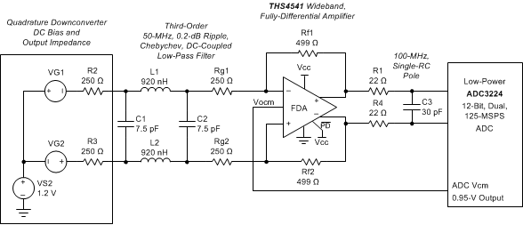
Operating the THS4541-Q1 with a DC-coupled differential input source is very simple and only requires that the input pins stay in range of the DC common-mode operating voltage. One example is a DC-to-50-MHz quadrature down-converter output. These outputs typically sit on a DC level with some internal source impedance to the external loads. The example of Figure 8-5 shows a design using the THS4541-Q1 with a simple, passive RLC filter to the inputs (the Rg elements act as the differential termination for the filter design). From the original source behind the internal 250-Ω outputs, this circuit is a gain of 1 to the THS4541-Q1 output pins. The DC common-mode operating voltage level shifts from the 1.2-V internal, to the mixer, to an output at the ADC Vcm voltage of 0.95 V. In this case, a simple average of the two DC voltages in the gain of 1 stage gives a 1.08-V input pin common-mode result that is well within range.
 Figure 8-5 Example DC-Coupled, Differential I/O Design from a Quadrature Mixer to an ADC