JAJSI65C November   2015  – October 2024 THS4541-Q1

PRODUCTION DATA  

  1.   1
  2. 特長
  3. アプリケーション
  4. 概要
  5. Device Comparison Table
  6. Pin Configuration and Functions
  7. Specifications
    1. 6.1 Absolute Maximum Ratings
    2. 6.2 ESD Ratings
    3. 6.3 Recommended Operating Conditions
    4. 6.4 Thermal Information
    5. 6.5 Electrical Characteristics: (Vs+) – Vs– = 5 V
    6. 6.6 Electrical Characteristics: (Vs+) – Vs– = 3 V
    7. 6.7 Typical Characteristics: 5-V Single Supply
    8. 6.8 Typical Characteristics: 3-V Single Supply
    9. 6.9 Typical Characteristics: 3-V to 5-V Supply Range
  8. Parameter Measurement Information
    1. 7.1 Example Characterization Circuits
    2. 7.2 Frequency-Response Shape Factors
    3. 7.3 I/O Headroom Considerations
    4. 7.4 Output DC Error and Drift Calculations and the Effect of Resistor Imbalances
    5. 7.5 Noise Analysis
    6. 7.6 Factors Influencing Harmonic Distortion
    7. 7.7 Driving Capacitive Loads
    8. 7.8 Thermal Analysis
  9. Detailed Description
    1. 8.1 Overview
      1. 8.1.1 Terminology and Application Assumptions
    2. 8.2 Functional Block Diagram
    3. 8.3 Feature Description
      1. 8.3.1 Differential I/O
      2. 8.3.2 Power-Down Control Pin ( PD)
        1. 8.3.2.1 Operating the Power Shutdown Feature
      3. 8.3.3 Input Overdrive Operation
    4. 8.4 Device Functional Modes
      1. 8.4.1 Operation from Single-Ended Sources to Differential Outputs
        1. 8.4.1.1 AC-Coupled Signal Path Considerations for Single-Ended Input to Differential Output Conversion
        2. 8.4.1.2 DC-Coupled Input Signal Path Considerations for Single-Ended to Differential Conversion
        3. 8.4.1.3 Resistor Design Equations for the Single-Ended to Differential Configuration of the FDA
        4. 8.4.1.4 Input Impedance for the Single-Ended to Differential FDA Configuration
      2. 8.4.2 Differential-Input to Differential-Output Operation
        1. 8.4.2.1 AC-Coupled, Differential-Input to Differential-Output Design Issues
        2. 8.4.2.2 DC-Coupled, Differential-Input to Differential-Output Design Issues
  10. Application and Implementation
    1. 9.1 Application Information
    2. 9.2 Typical Applications
      1. 9.2.1 Designing Attenuators
        1. 9.2.1.1 Design Requirements
        2. 9.2.1.2 Detailed Design Procedure
        3. 9.2.1.3 Application Curve
      2. 9.2.2 Interfacing to High-Performance ADCs
        1. 9.2.2.1 Design Requirements
        2. 9.2.2.2 Detailed Design Procedure
        3. 9.2.2.3 Application Curve
    3. 9.3 Power Supply Recommendations
    4. 9.4 Layout
      1. 9.4.1 Layout Guidelines
      2. 9.4.2 Layout Example
  11. 10Device and Documentation Support
    1. 10.1 Device Support
      1. 10.1.1 Development Support
        1. 10.1.1.1 TINA Simulation Model Features
    2. 10.2 Documentation Support
      1. 10.2.1 Related Documentation
    3. 10.3 ドキュメントの更新通知を受け取る方法
    4. 10.4 サポート・リソース
    5. 10.5 Trademarks
    6. 10.6 静電気放電に関する注意事項
    7. 10.7 用語集
  12. 11Revision History
  13. 12Mechanical, Packaging, and Orderable Information

パッケージ・オプション

メカニカル・データ(パッケージ|ピン)
サーマルパッド・メカニカル・データ
発注情報

Typical Characteristics: 3-V Single Supply

at Vs+ = 3 V, Vs– = GND, Vocm is open, 50-Ω single-ended input to differential output, gain = 2 V/V, Rload = 500 Ω, and TA ≈ 25°C (unless otherwise noted)
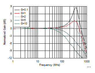
THS4541-Q1 Small-Signal Frequency Response vs Gain
Rf = 402 Ω, Vout = 100 mVPP, see Figure 7-1 and Table 8-1 for resistor values
Figure 6-19 Small-Signal Frequency Response vs Gain
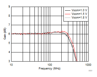
THS4541-Q1 Small-Signal Frequency response vs Vocm
Vout = 100 mVPP, see Figure 7-1 with Vocm adjusted
Figure 6-21 Small-Signal Frequency response vs Vocm
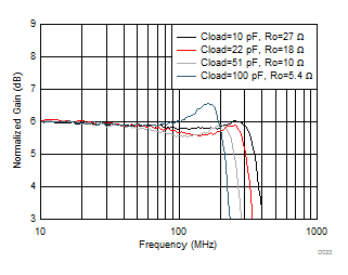
THS4541-Q1 Small-Signal Frequency Response vs Cload
100 mVPP at load, Av = 2 (see Figure 7-11), two series Ro added at output before Cload
Figure 6-23 Small-Signal Frequency Response vs Cload
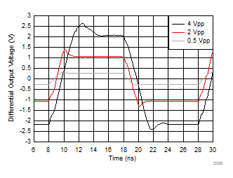
THS4541-Q1 Small- and Large-Signal Step Response
50-MHz input, 0.3-ns input edge rate, single-ended input to differential output, DC coupled, see Figure 7-3
Figure 6-25 Small- and Large-Signal Step Response
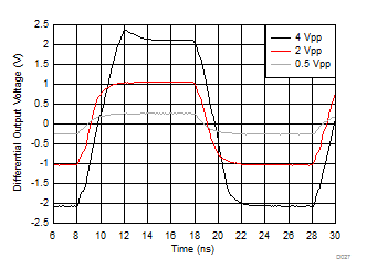
THS4541-Q1 Small- and Large-Signal Step Response
G = 5 V/V, 50-MHz input, 0.3-ns input edge rate, single-ended input to differential output, see Figure 7-3
Figure 6-27 Small- and Large-Signal Step Response
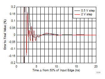
THS4541-Q1 Small- and Large-Signal Step Settling Time
Simulated with 2-ns input transition time,
see Figure 7-3
Figure 6-29 Small- and Large-Signal Step Settling Time
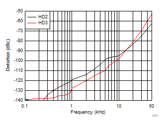
THS4541-Q1 Harmonic Distortion Over Frequency
2-VPP output, see Figure 7-1 with Vs+ = 3 V, Vocm = 1.5 V
Figure 6-31 Harmonic Distortion Over Frequency
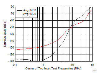
THS4541-Q1 IMD2 and IM3 Over Frequency
1 VPP each tone, see Figure 7-1 with Vs+ = 3 V, Vocm = 1.5 V
Figure 6-33 IMD2 and IM3 Over Frequency
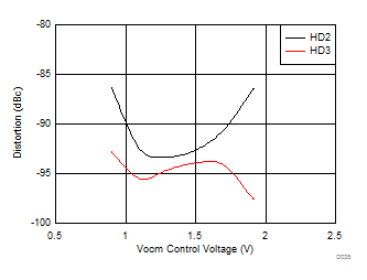
THS4541-Q1 Harmonic Distortion vs Vocm
f = 10 MHz, 2-VPP output,
ee Figure 7-3 with Vocm adjusted
Figure 6-35 Harmonic Distortion vs Vocm
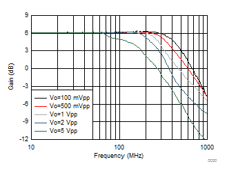
THS4541-Q1 Frequency Response vs Vopp
See Figure 7-1 with VCC = 3 V and Vocm = 1.5 V
 
Figure 6-20 Frequency Response vs Vopp
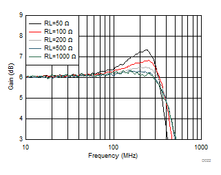
THS4541-Q1 Small-Signal Frequency Response vs Rload
Vout = 100 mVPP, see Figure 7-1 with the Rload adjusted
Figure 6-22 Small-Signal Frequency Response vs Rload
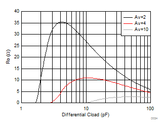
THS4541-Q1 Recommended Ro vs Cload
Two Ro at output to differential Cload in parallel with 500 Ω, see Figure 7-11 and Table 8-1
Figure 6-24 Recommended Ro vs Cload
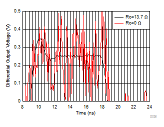
THS4541-Q1 Step
                        Response Into Capacitive Load
500-mVPP output into 22-pF Cload, see Figure 7-11
with Vs+ = 3 V and Vocm = 1.5 V
Figure 6-26 Step Response Into Capacitive Load
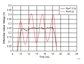
THS4541-Q1 Step Response into Capacitive Load
G = 5 V/V, 500-mVpp output into 22-pF Cload, see Figure 7-11 and Table 8-1
Figure 6-28 Step Response into Capacitive Load
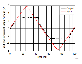
THS4541-Q1 Overdrive Recovery Performance
Single-ended to differential gain of 2 (see Figure 7-3),
> 2 × input overdrive
Figure 6-30 Overdrive Recovery Performance
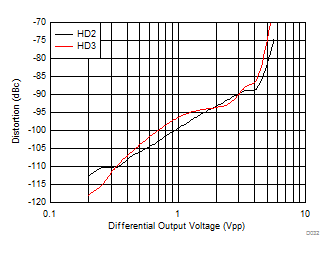
THS4541-Q1 Harmonic Distortion vs Output Swing
f = 10 MHz, see Figure 7-1 with Vs+ = 3 V, Vocm = 1.5 V
Figure 6-32 Harmonic Distortion vs Output Swing
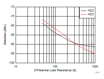
THS4541-Q1 Harmonic Distortion vs Rload
f = 10 MHz, see Figure 7-1 with Vs+ = 3 V, Vocm = 1.5 V
Figure 6-34 Harmonic Distortion vs Rload
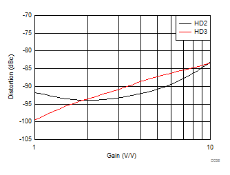
THS4541-Q1 Harmonic Distortion vs Gain
f = 10 MHz, 2-VPP output,
see Figure 7-1 and Table 8-1 for gain setting
Figure 6-36 Harmonic Distortion vs Gain