JAJSL64D April   2016  – June 2021 THS4551

PRODUCTION DATA  

  1. 特長
  2. アプリケーション
  3. 概要
  4. Revision History
  5. Companion Devices
  6. Pin Configuration and Functions
  7. Specifications
    1. 7.1 Absolute Maximum Ratings
    2. 7.2 ESD Ratings
    3. 7.3 Recommended Operating Conditions
    4. 7.4 Thermal Information
    5. 7.5 Electrical Characteristics: (VS+) – (VS–) = 5 V
    6. 7.6 Electrical Characteristics: (VS+) – (VS–) = 3 V
    7. 7.7 Typical Characteristics: (VS+) – (VS–) = 5 V
    8. 7.8 Typical Characteristics: (VS+) – (VS–) = 3 V
    9. 7.9 Typical Characteristics: 3-V to 5-V Supply Range
  8. Parameter Measurement Information
    1. 8.1 Example Characterization Circuits
    2. 8.2 Output Interface Circuit for DC-Coupled Differential Testing
    3. 8.3 Output Common-Mode Measurements
    4. 8.4 Differential Amplifier Noise Measurements
    5. 8.5 Balanced Split-Supply Versus Single-Supply Characterization
    6. 8.6 Simulated Characterization Curves
    7. 8.7 Terminology and Application Assumptions
  9. Detailed Description
    1. 9.1 Overview
    2. 9.2 Functional Block Diagram
    3. 9.3 Feature Description
      1. 9.3.1 Differential Open-Loop Gain and Output Impedance
      2. 9.3.2 Setting Resistor Values Versus Gain
      3. 9.3.3 I/O Headroom Considerations
      4. 9.3.4 Output DC Error and Drift Calculations and the Effect of Resistor Imbalances
    4. 9.4 Device Functional Modes
      1. 9.4.1 Operation from Single-Ended Sources to Differential Outputs
        1. 9.4.1.1 AC-Coupled Signal Path Considerations for Single-Ended Input to Differential Output Conversions
        2. 9.4.1.2 DC-Coupled Input Signal Path Considerations for Single-Ended to Differential Conversions
      2. 9.4.2 Operation from a Differential Input to a Differential Output
        1. 9.4.2.1 AC-Coupled, Differential-Input to Differential-Output Design Issues
        2. 9.4.2.2 DC-Coupled, Differential-Input to Differential-Output Design Issues
      3. 9.4.3 Input Overdrive Performance
  10. 10Application and Implementation
    1. 10.1 Application Information
      1. 10.1.1 Noise Analysis
      2. 10.1.2 Factors Influencing Harmonic Distortion
      3. 10.1.3 Driving Capacitive Loads
      4. 10.1.4 Interfacing to High-Performance Precision ADCs
      5. 10.1.5 Operating the Power Shutdown Feature
      6. 10.1.6 Designing Attenuators
      7. 10.1.7 The Effect of Adding a Feedback Capacitor
    2. 10.2 Typical Applications
      1. 10.2.1 An MFB Filter Driving an ADC Application
        1. 10.2.1.1 Design Requirements
        2. 10.2.1.2 Detailed Design Procedure
        3. 10.2.1.3 Application Curves
      2. 10.2.2 Differential Transimpedance Output to a High-Grade Audio PCM DAC Application
        1. 10.2.2.1 Design Requirements
        2. 10.2.2.2 Detailed Design Procedure
        3. 10.2.2.3 Application Curves
      3. 10.2.3 ADC3k Driver with a 2nd-Order RLC Interstage Filter Application
        1. 10.2.3.1 Design Requirements
        2. 10.2.3.2 Detailed Design Procedure
        3. 10.2.3.3 Application Curve
  11. 11Power Supply Recommendations
    1. 11.1 Thermal Analysis
  12. 12Layout
    1. 12.1 Layout Guidelines
      1. 12.1.1 Board Layout Recommendations
    2. 12.2 Layout Example
    3. 12.3 EVM Board
  13. 13Device and Documentation Support
    1. 13.1 Device Support
      1. 13.1.1 TINA-TI Simulation Model Features
    2. 13.2 Documentation Support
      1. 13.2.1 Related Documentation
    3. 13.3 Receiving Notification of Documentation Updates
    4. 13.4 サポート・リソース
    5. 13.5 Trademarks
    6. 13.6 Electrostatic Discharge Caution
    7. 13.7 Glossary
  14. 14Mechanical, Packaging, and Orderable Information

パッケージ・オプション

メカニカル・データ(パッケージ|ピン)
サーマルパッド・メカニカル・データ
発注情報

Application Curve

Driving a 2-MHz ±0.2-V square wave into this circuit (using a TINA-TI™ simulation file for the circuit of Figure 10-17) gives the response shown in Figure 10-18 at the ADC. The red trace is a –1-dBFS, 1.8-VPP square wave at the ADC input pins. The gray trace is the input signal at the RT termination resistor. The black trace is the common-mode voltage at the FDA input pins. Note that the input pin voltage swing stays above ground and in range for this bipolar input, single, 3.3-V supply design.
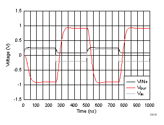
GUID-0673603A-CC9B-49D6-8358-1DDC2C555C15-low.gifFigure 10-18 Time-Domain Waveform

Unbuffered pipeline ADCs draw a clock-rate-dependent input common-mode current. For the ADC3241, this input current is specified as 1.5 µA per MSPS. Operating at 25 MSPS, the common-mode current drops the common-mode voltage from 0.95 V at the THS4551 outputs by 37.5 µA × 45.8 Ω = 1.7 mV to 0.9483 V. This value is well within the allowed ±25-mV common-mode deviation from the ADC VCM output. Consider this effect carefully when using higher resistor values in the interface at the ADC.