JAJSIB3D August   2017  – February 2021 THS4561

PRODUCTION DATA  

  1. 特長
  2. アプリケーション
  3. 概要
  4. Revision History
  5. Device Comparison Table
  6. Pin Configuration and Functions
  7. Specifications
    1. 7.1 Absolute Maximum Ratings
    2. 7.2 ESD Ratings
    3. 7.3 Recommended Operating Conditions
    4. 7.4 Thermal Information
    5. 7.5 Electrical Characteristics: VS+ – VS– = 5 V to 12 V
    6. 7.6 Typical Characteristics: (VS+) – (VS–) = 12 V
    7. 7.7 Typical Characteristics: (VS+) – (VS–) = 5 V
    8. 7.8 Typical Characteristics: (VS+) – (VS–) = 3 V
    9. 7.9 Typical Characteristics: (VS+) – (VS–) = 3-V to 12-V Supply Range
  8. Parameter Measurement Information
    1. 8.1 Example Characterization Circuits
    2. 8.2 Output Interface Circuit for DC-Coupled Differential Testing
    3. 8.3 Output Common-Mode Measurements
    4. 8.4 Differential Amplifier Noise Measurements
    5. 8.5 Balanced Split-Supply Versus Single-Supply Characterization
    6. 8.6 Simulated Characterization Curves
    7. 8.7 Terminology and Application Assumptions
  9. Detailed Description
    1. 9.1 Overview
    2. 9.2 Functional Block Diagram
    3. 9.3 Feature Description
    4. 9.4 Device Functional Modes
      1. 9.4.1 Power-Down Mode
      2. 9.4.2 Single-Ended Source to Differential Output Mode
        1. 9.4.2.1 AC-Coupled Signal Path Considerations for Single-Ended Input to Differential Output Conversions
        2. 9.4.2.2 DC-Coupled Input Signal Path Considerations for Single-Ended to Differential Conversions
      3. 9.4.3 Differential Input to a Differential Output Mode
        1. 9.4.3.1 AC-Coupled, Differential-Input to Differential-Output Design Issues
  10. 10Application and Implementation
    1. 10.1 Application Information
      1. 10.1.1 Differential Open-Loop Gain and Output Impedance
      2. 10.1.2 Setting Resistor Values Versus Gain
      3. 10.1.3 Noise Analysis
      4. 10.1.4 Factors Influencing Harmonic Distortion
      5. 10.1.5 Input Overdrive Performance
    2. 10.2 Typical Application
      1. 10.2.1 Design Requirements
      2. 10.2.2 Detailed Design Procedure
      3. 10.2.3 Application Curves
  11. 11Power Supply Recommendations
  12. 12Layout
    1. 12.1 Layout Guidelines
      1. 12.1.1 Board Layout Recommendations
    2. 12.2 Layout Examples
  13. 13Device and Documentation Support
    1. 13.1 ドキュメントの更新通知を受け取る方法
    2. 13.2 サポート・リソース
    3. 13.3 Trademarks
    4. 13.4 静電気放電に関する注意事項
    5. 13.5 用語集
  14. 14Mechanical, Packaging, and Orderable Information

パッケージ・オプション

メカニカル・データ(パッケージ|ピン)
サーマルパッド・メカニカル・データ
発注情報

Typical Characteristics: (VS+) – (VS–) = 5 V

at TA ≈ 25°C, VOCM pin = open, RF = 1.5 kΩ, RL = 1 kΩ, VO = 2 VPP, 50-Ω input match, G = 1 V/V, PD = VS+, single-ended input (SE-in), differential output (diff-out), and input and output referenced to default midsupply for AC-coupled tests (unless otherwise noted); see Figure 8-1 for a gain of 1-V/V test circuit.

GUID-78F32750-234D-4FD8-91B0-98918074E4A7-low.gif
VO = 200 mVPP, see Figure 8-1 and Table 10-1 for resistor values
Figure 7-15 Small-Signal Frequency Response vs Gain
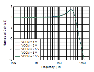
GUID-9495C9A4-41F4-4262-987F-CD029F70CC2E-low.gif
VO = 200 mVPP, see Figure 8-1 with VOCM adjusted
Figure 7-17 Small-Signal Frequency Response vs VOCM
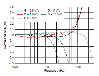
GUID-9FB96CA0-480A-4D9B-ADC1-C568EE057625-low.gif
VO = 200 mVPP
Figure 7-19 Gain Flatness vs Frequency
GUID-8A5890D4-E41D-4D05-A688-AC83FAC28F8F-low.gifFigure 7-21 Harmonic Distortion vs Frequency
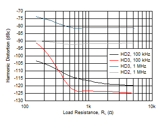
GUID-2E5F3935-7845-4F36-9958-36261924EE66-low.gif
VO = 5 VPP with RL adjusted
Figure 7-23 Harmonic Distortion vs RL
GUID-26A1C0D5-AEEE-429A-8866-168DBCF1DD8E-low.gif
VO = 5 VPP with VOCM adjusted
Figure 7-25 Harmonic Distortion vs VOCM
GUID-63E322AD-1EDC-47FD-A22E-4E570E9AA260-low.gif
VO = 2-V step,
SE-in, diff-out: rising SR = 325 V/µs, falling SR = 230 V/µs,
diff-in, diff-out: rising SR = 305 V/µs, falling SR = 310 V/µs
Figure 7-27 Large-Signal Step Response
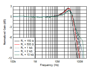
GUID-95EEAE30-C700-4EF2-A0A5-99EF27F2993E-low.gifFigure 7-16 Frequency Response vs VO
GUID-4D7F7DF8-9F7F-4A82-8CEA-B03C99E9745D-low.gif
VO = 200 mVPP, see Figure 8-1 with RL adjusted
Figure 7-18 Small-Signal Frequency Response vs RL
GUID-F7B6904F-C2AE-492A-84FE-4B51A904B5E4-low.gif
1/f corners: en = 8 Hz, in = 700 Hz
Figure 7-20 Input Noise Density vs Frequency
GUID-066182E9-F1D8-48E0-AF61-C1F75B0765EF-low.gifFigure 7-22 Harmonic Distortion vs VO
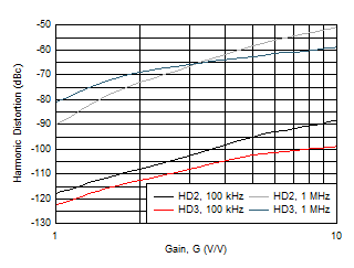
GUID-A3CA2056-BCDA-4C8E-A6A4-F27A7D47EA04-low.gif
VO = 5 VPP, see Table 10-1 for gain setting
Figure 7-24 Harmonic Distortion vs Gain
GUID-6773BEE1-C506-473C-83E4-22FF3F79FFA7-low.gif
VO = 2 VPP per tone, ±50-kHz tone spacing
Figure 7-26 Intermodulation Distortion (IMD2 and IMD3) vs Frequency
GUID-05FECB88-E5AE-4BA4-B477-040A4DC13B0A-low.gif
VS = 5 V, VOCM at midsupply, average of 30 units
Figure 7-28 ±Maximum Output Voltage vs Output Current and Temperature