JAJSIB3D August   2017  – February 2021 THS4561

PRODUCTION DATA  

  1. 特長
  2. アプリケーション
  3. 概要
  4. Revision History
  5. Device Comparison Table
  6. Pin Configuration and Functions
  7. Specifications
    1. 7.1 Absolute Maximum Ratings
    2. 7.2 ESD Ratings
    3. 7.3 Recommended Operating Conditions
    4. 7.4 Thermal Information
    5. 7.5 Electrical Characteristics: VS+ – VS– = 5 V to 12 V
    6. 7.6 Typical Characteristics: (VS+) – (VS–) = 12 V
    7. 7.7 Typical Characteristics: (VS+) – (VS–) = 5 V
    8. 7.8 Typical Characteristics: (VS+) – (VS–) = 3 V
    9. 7.9 Typical Characteristics: (VS+) – (VS–) = 3-V to 12-V Supply Range
  8. Parameter Measurement Information
    1. 8.1 Example Characterization Circuits
    2. 8.2 Output Interface Circuit for DC-Coupled Differential Testing
    3. 8.3 Output Common-Mode Measurements
    4. 8.4 Differential Amplifier Noise Measurements
    5. 8.5 Balanced Split-Supply Versus Single-Supply Characterization
    6. 8.6 Simulated Characterization Curves
    7. 8.7 Terminology and Application Assumptions
  9. Detailed Description
    1. 9.1 Overview
    2. 9.2 Functional Block Diagram
    3. 9.3 Feature Description
    4. 9.4 Device Functional Modes
      1. 9.4.1 Power-Down Mode
      2. 9.4.2 Single-Ended Source to Differential Output Mode
        1. 9.4.2.1 AC-Coupled Signal Path Considerations for Single-Ended Input to Differential Output Conversions
        2. 9.4.2.2 DC-Coupled Input Signal Path Considerations for Single-Ended to Differential Conversions
      3. 9.4.3 Differential Input to a Differential Output Mode
        1. 9.4.3.1 AC-Coupled, Differential-Input to Differential-Output Design Issues
  10. 10Application and Implementation
    1. 10.1 Application Information
      1. 10.1.1 Differential Open-Loop Gain and Output Impedance
      2. 10.1.2 Setting Resistor Values Versus Gain
      3. 10.1.3 Noise Analysis
      4. 10.1.4 Factors Influencing Harmonic Distortion
      5. 10.1.5 Input Overdrive Performance
    2. 10.2 Typical Application
      1. 10.2.1 Design Requirements
      2. 10.2.2 Detailed Design Procedure
      3. 10.2.3 Application Curves
  11. 11Power Supply Recommendations
  12. 12Layout
    1. 12.1 Layout Guidelines
      1. 12.1.1 Board Layout Recommendations
    2. 12.2 Layout Examples
  13. 13Device and Documentation Support
    1. 13.1 ドキュメントの更新通知を受け取る方法
    2. 13.2 サポート・リソース
    3. 13.3 Trademarks
    4. 13.4 静電気放電に関する注意事項
    5. 13.5 用語集
  14. 14Mechanical, Packaging, and Orderable Information

パッケージ・オプション

メカニカル・データ(パッケージ|ピン)
サーマルパッド・メカニカル・データ
発注情報

Typical Characteristics: (VS+) – (VS–) = 3-V to 12-V Supply Range

at TA ≈ 25°C, VOCM pin = open, RF = 1.5 kΩ, RL = 1 kΩ, VO = 2 VPP, 50-Ω input match, G = 1 V/V, PD = VS+, single-ended input, differential output, and input and output referenced to default midsupply for AC-coupled tests (unless otherwise noted); see Figure 8-1 for a gain of 1-V/V test circuit.
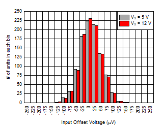
GUID-01F82CCE-4D20-4AE6-859A-9F20811937FC-low.gif
1000 DGK units at each VS
Figure 7-35 Input Offset Voltage (VOS)
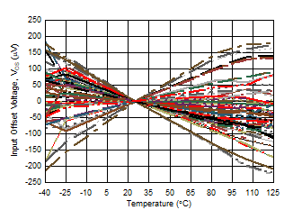
GUID-54AA24BB-B556-495F-A2DE-3E5619DC292C-low.gif
VS = 12 V, 5 V, and 3 V,
delta from 25°C VOS, 30 DGK units for each VS
Figure 7-37 Input Offset Voltage vs Temperature
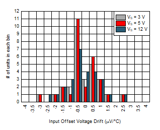
GUID-4555E6D1-B20D-4432-8FF9-79642BC00643-low.gif
–40°C to +125°C endpoint drift, 30 DGK units for each VS
Figure 7-39 Input Offset Voltage Drift Histogram
GUID-F024FF18-D285-4938-B008-F093681F48B8-low.gif
Simulated
Figure 7-41 Main Amplifier Differential Open-Loop Gain and Phase vs Frequency
GUID-EC00BF09-ABD2-4CA3-8ED1-B939870145FC-low.gif
Figure 7-43 Closed-Loop Output Impedance vs Frequency
GUID-01F0CFAE-360D-4B6C-BBFA-0233926A4EE2-low.gif
Average of 30 units
Figure 7-45 Quiescent Current vs VS
GUID-9E86CF00-6B9E-46D2-A1C5-1B548934757A-low.gif
Figure 7-47 Common-Mode Voltage, Small-Signal and Large-Signal Response (VOCM Pin Driven)
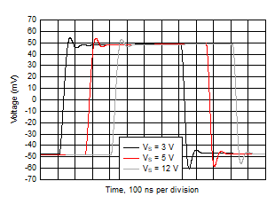
GUID-10C07646-D4F8-4200-A7B1-BF18D4D3F17A-low.gif
VOCM pin driven, 0.1-V VOCM step
Figure 7-49 Common-Mode Voltage Small-Signal Step Response
GUID-1BB9DFB5-7F9B-400E-ADA4-BB870A95D74A-low.gif
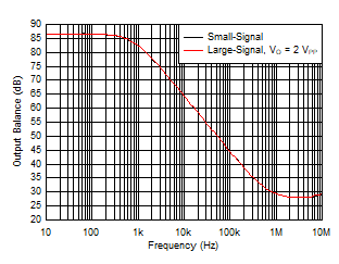
Simulated
Figure 7-51 Output Balance vs Frequency
GUID-B516E4A4-A41E-47E7-B61C-8C96155AD730-low.gif
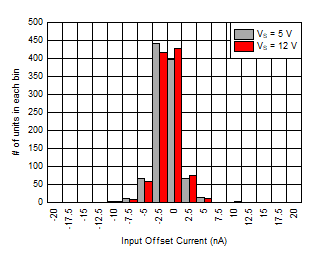
1000 DGK units at each VS
Figure 7-36 Input Offset Current (IOS)
GUID-3185E7C0-F1C1-424F-A870-84C94E798289-low.gif
VS = 12 V and 5 V,
delta from 25°C IOS, 50 DGK units for each VS
Figure 7-38 Input Offset Current vs Temperature
GUID-BB07A59D-FC32-4EAA-8E62-9B38232B10F3-low.gif
–40°C to +125°C endpoint drift, 50 DGK units for each VS
Figure 7-40 Input Offset Current Drift Histogram
GUID-DE26BCB2-A4AF-494E-9343-BCCDA235B58C-low.gif
Simulated
Figure 7-42 Open-Loop Output Impedance vs Frequency
GUID-1CDA989D-FCD8-4A91-A76D-F79718643ABE-low.gif
VO = 100-mV step, tr (10% - 90%) = 5.7 ns
Figure 7-44 Small-Signal Step Response
GUID-44DBA810-11C2-4333-8A8F-CDDC3C687813-low.gif
5 MHz, 2-VPP input, G = 1 V/V, see Figure 8-1
Figure 7-46 PD Turnon and Turnoff Waveform
GUID-8D2ADF8B-5A79-42EE-BB51-2477C01FBA93-low.gif
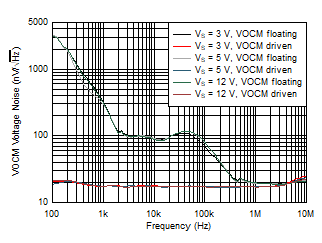
The VOCM pin is either driven to midsupply by low-impedance source or allowed to float and default to midsupply
Figure 7-48 Output Common-Mode (VOCM) Noise vs Frequency
GUID-66AEB325-B988-4BFF-A0DC-89BA8C269033-low.gif
VOCM pin driven, 1-V VOCM step
Figure 7-50 Common-Mode Voltage Large-Signal Step Response
GUID-51EDD667-E09E-4D2B-A70F-1AE5C12A05AE-low.gif
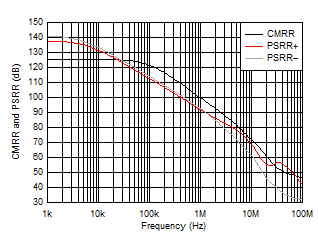
Simulated
Figure 7-52 CMRR and PSRR vs Frequency