JAJSC60F April 2016 – June 2024 THS6212
PRODUCTION DATA
- 1
- 1 特長
- 2 アプリケーション
- 3 概要
- 4 Pin Configuration and Functions
- 5 Specifications
- 6 Detailed Description
- 7 Application and Implementation
- 8 Device and Documentation Support
- 9 Revision History
- 10Mechanical, Packaging, and Orderable Information
パッケージ・オプション
デバイスごとのパッケージ図は、PDF版データシートをご参照ください。
メカニカル・データ(パッケージ|ピン)
- RHF|24
サーマルパッド・メカニカル・データ
発注情報
7.2.1.2 Detailed Design Procedure
For ease of test purposes in this design, the THS6212 input impedance is set to 50 Ω with a resistor to ground and the output impedance is set to 50 Ω with a series output resistor. Voltage swings reported in the Electrical Characteristics tables are taken directly at the input and output pins, whereas load powers (dBm) are defined at a matched 50-Ω load. For the circuit of Figure 7-1, the total effective load is 100 Ω || 1.24 kΩ || 1.24 kΩ = 86.1 Ω. This approach allows a source termination impedance to be set at the input that is independent of the signal gain. For instance, simple differential filters can be included in the signal path right up to the noninverting inputs with no interaction with the gain setting. The differential signal gain for the circuit of Figure 7-1 is given by Equation 5:
where
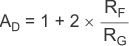
- AD = differential gain
A value of 274 Ω for the AD = 10-V/V design is given by Figure 7-1. The device bandwidth is primarily controlled with the feedback resistor value because the THS6212 is a current-feedback (CFB) amplifier; the differential gain, however, can be adjusted with considerable freedom using just the RG resistor. In fact, RG can be reduced by a reactive network that provides a very isolated shaping to the differential frequency response.
Various combinations of single-supply or ac-coupled gain can also be delivered using the basic circuit of Figure 7-1. Common-mode bias voltages on the two noninverting inputs pass on to the output with a gain of 1 V/V because an equal dc voltage at each inverting node does not create current through RG. This circuit does show a common-mode gain of 1 V/V from the input to output. The source connection must either remove this common-mode signal if undesired (using an input transformer can provide this function), or the common-mode voltage at the inputs can be used to set the output common-mode bias. If the low common-mode rejection of this circuit is a problem, the output interface can also be used to reject that common-mode signal. For instance, most modern differential input analog-to-digital converters (ADCs) reject common-mode signals very well, and a line-driver application through a transformer also attenuates the common-mode signal through to the line.