JAJSC60F April 2016 – June 2024 THS6212
PRODUCTION DATA
- 1
- 1 特長
- 2 アプリケーション
- 3 概要
- 4 Pin Configuration and Functions
- 5 Specifications
- 6 Detailed Description
- 7 Application and Implementation
- 8 Device and Documentation Support
- 9 Revision History
- 10Mechanical, Packaging, and Orderable Information
パッケージ・オプション
デバイスごとのパッケージ図は、PDF版データシートをご参照ください。
メカニカル・データ(パッケージ|ピン)
- RHF|24
サーマルパッド・メカニカル・データ
発注情報
6.3.1 Output Voltage and Current Drive
The THS6212 provides output voltage and current capabilities that are unsurpassed in a low-cost, monolithic op amp. The output voltage (under no load at room temperature) typically swings closer than 1.1 V to either supply rail and typically swings to within 1.1 V of either supply with a 100 Ω differential load. The THS6212 can deliver over 350 mA of current with a 25 Ω load.
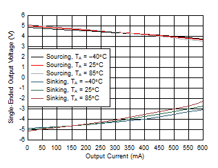
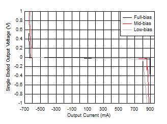
Good thermal design of the system is important, including use of heat sinks and active cooling methods, if the THS6212 is pushed to the limits of the output drive capabilities. Figure 6-1 and Figure 6-2 show the output drive of the THS6212 under two different sets of conditions where TA is approximately equal to TJ. In practical applications, TJ is often much higher than TA and highly depends on the device configuration, signal parameters, and PCB thermal design. To represent the full output drive capability of the THS6212 in Figure 6-1 and Figure 6-2, TJ ≈ TA is achieved by pulsing or sweeping the output current for a duration of less than 100 ms.

| VS = 12 V, TJ ≈ TA |

| VS = 12 V, TJ ≈ TA ≈ 25°C |
In Figure 6-1, the output voltages are differentially slammed to the rail and the output current is single-endedly sourced or sunk using a source measure unit (SMU) for less than 100 ms. The single-ended output voltage of each output is then measured prior to removing the load current. After removing the load current, the outputs are brought back to mid-supply before repeating the measurement for different load currents. This entire process is repeated for each ambient temperature. Under the slammed output voltage condition of Figure 6-1, the output transistors are in saturation and the transistors start going into linear operation as the output swing is backed off for a given IO,
In Figure 6-2, the inputs are floated and the output voltages are allowed to settle to the mid-supply voltage. The load current is then single-endedly swept for sourcing (greater than 0 mA) and sinking (less than 0 mA) conditions and the single-ended output voltage is measured at each current-forcing condition. The current sweep is completed in a few seconds (approximately 3 to 4 seconds) so as not to significantly raise the junction temperature (TJ) of the device from the ambient temperature (TA). The output is not swinging and the output transistors are in linear operation in Figure 6-2 until the current drawn exceeds the device capabilities, at which point the output voltage starts to deviate quickly from the no load output voltage.
To maintain maximum output stage linearity, output short-circuit protection is not provided. This absence of short-circuit protection is normally not a problem because most applications include a series-matching resistor at the output that limits the internal power dissipation if the output side of this resistor is shorted to ground. However, shorting the output pin directly to the adjacent positive power-supply pin, in most cases, permanently damages the amplifier.