at TA ≈ 25°C, AV
= 10 V/V, RF = 1.24 kΩ, RL = 50 Ω, RS = 2.5 Ω,
RADJ = 0 Ω, full-bias mode, and VCM = open (unless otherwise
noted)
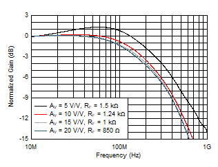
 Figure 5-1 Small-Signal Frequency Response
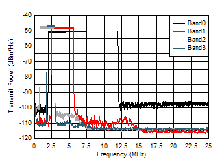
 Figure 5-3 Out-of-Band Suppression
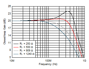
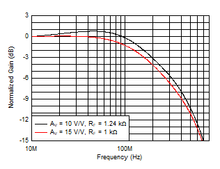
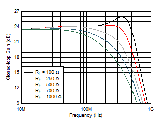
 Figure 5-5 Small-Signal Frequency Response vs RF
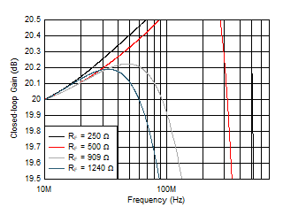
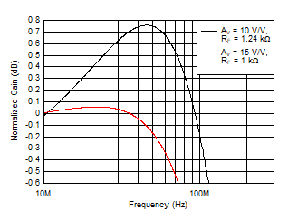
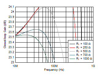
 Figure 5-7 Small-Signal Gain Flatness vs RF
 Figure 5-9 Large-Signal Gain Flatness
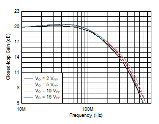
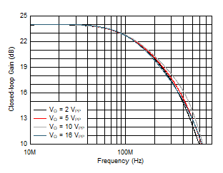
 Figure 5-11 Large-Signal Frequency Response vs VO
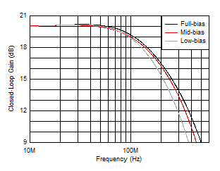
 Figure 5-13 Small-Signal Frequency Response vs Bias Modes
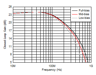
 Figure 5-15 Large-Signal Frequency Response vs Bias Modes
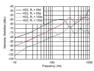
 Figure 5-17 Harmonic Distortion vs Frequency
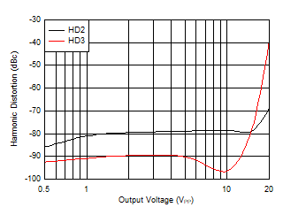
 Figure 5-19 Harmonic Distortion vs VO
| f =
1 MHz, VO = 2 VPP, AV =
10 V/V |
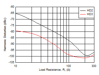
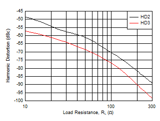
Figure 5-21 Harmonic Distortion vs RL
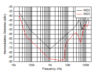
| ±12.2 kHz tone spacing, VO = 2
VPP per tone |
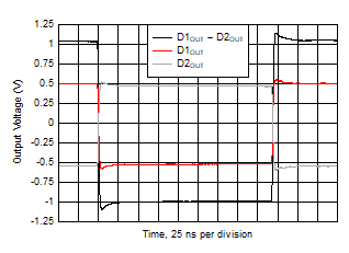
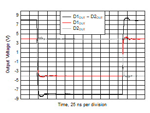
Figure 5-23 Intermodulation Distortion vs Frequency Figure 5-25 Small-Signal Pulse Response
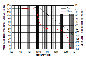
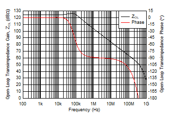
 Figure 5-27 Open-Loop Transimpedance Gain and Phase vs Frequency
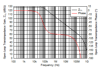
 Figure 5-29 Open-Loop Transimpedance Gain and Phase vs Frequency
| RL = no load, average of 30
devices |
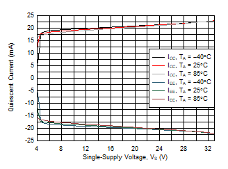
Figure 5-31 Quiescent Current vs Single-Supply Voltage
| RL = no load, average of 30
devices |
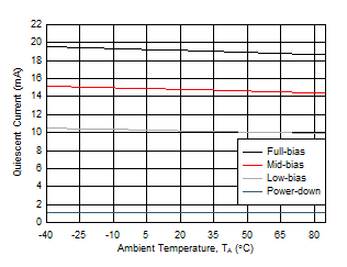
Figure 5-33 Quiescent Current vs Temperature
| B1 =
full-bias to mid-bias transition with B2 = DGND, B2 =
full-bias to low-bias transition with B1 = DGND, DGND =
VS– |
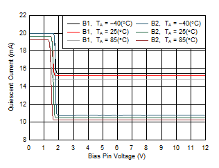
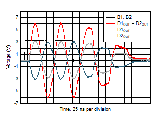
Figure 5-35 Mode
Transition Voltage Threshold Figure 5-2 Large-Signal Frequency Response
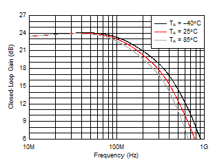
 Figure 5-4 Small-Signal Frequency Response vs Temperature
 Figure 5-6 Small-Signal Frequency Response vs RF
 Figure 5-8 Small-Signal Gain Flatness vs RF
| VO = 100 mVPP |
| Frequency response is measured at the device output pin
before the isolation resistor. |
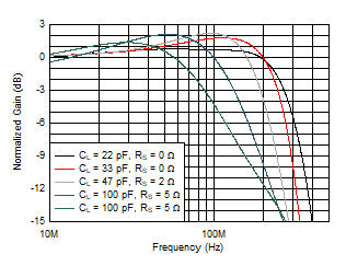
Figure 5-10 Small-Signal Frequency Response vs CLOAD Figure 5-12 Large-Signal Frequency Response vs VO
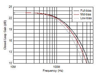
 Figure 5-14 Small-Signal Frequency Response vs Bias Modes
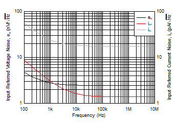
 Figure 5-16 Input
Voltage and Current Noise Density vs Frequency
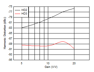
 Figure 5-18 Harmonic Distortion vs Gain
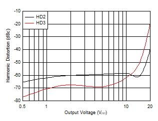
 Figure 5-20 Harmonic Distortion vs VO
| f =
10 MHz, VO = 2 VPP, AV
= 10 V/V |
Figure 5-22 Harmonic Distortion vs RL
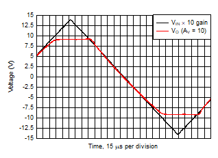
| VIN
= 2.8-VPP triangular waveform |
Figure 5-24 Overdrive Recovery Figure 5-26 Large-Signal Pulse Response
 Figure 5-28 Open-Loop Transimpedance Gain and Phase vs Frequency
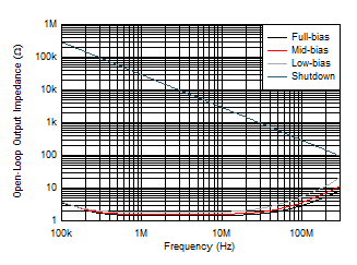
 Figure 5-30 Open-Loop Output Impedance vs Frequency
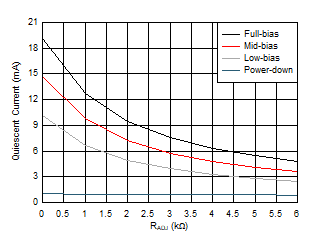
 Figure 5-32 Quiescent Current vs RADJ
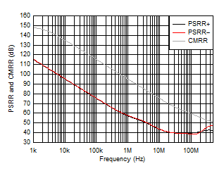
 Figure 5-34 PSRR
and CMRR vs Frequency
 Figure 5-36 Full-Bias and Shutdown Mode Transition Timing
