SBOS643A April 2014 – May 2014 THS6226A
PRODUCTION DATA.
- 1 Features
- 2 Applications
- 3 Description
- 4 Revision History
- 5 Pin Configuration and Functions
- 6 Specifications
- 7 Detailed Description
- 8 Applications and Implementation
- 9 Power Supply Recommendations
- 10Layout
- 11Device and Documentation Support
- 12Mechanical, Packaging, and Orderable Information
パッケージ・オプション
メカニカル・データ(パッケージ|ピン)
- RHB|32
サーマルパッド・メカニカル・データ
- RHB|32
発注情報
1 Features
- Digitally-Adjustable Quiescent Current:
9.4 mA to 24.8 mA - Bias Current Step: 1.0 mA
- Independent Voltage Boost and Main Line Driver Disable
- Low-Power Line Termination Mode
- Full Capacitor Recharge: 200 µs
- Low Input Voltage Noise Density:
6.5 nV/√Hz Input-Referred Voltage Noise - Low MTPR Distortion:
70 dB with +19.8 dBm G.993.2—Profile 8b - –83-dBc HD3 (1 MHz, 60-Ω Differential)
- High Output Current: 383 mA into 60 Ω
- Wide Output Swing: 40 VPP (+12-V, 60-Ω Differential Load with a 1:1.4 Transformer)
- Wide Bandwidth: 97 MHz
- Port-to-Port Separation: 90 dB at 1 MHz
- PSRR: 70 dB at 1 MHz for Good Isolation
2 Applications
- Ideal for All VDSL2 Profiles
- Backwards-Compatible with ADSL, ADSL2+, and ADSL2++ Systems
3 Description
The THS6226A is a dual-port, class H, current-feedback architecture, differential line driver amplifier system ideal for xDSL systems. The device is targeted for use in very-high-bit-rate digital subscriber line 2 (VDSL2) line driver systems that enable native DTM signals while supporting greater than 20.5-dBm line power (up to 8.5 MHz) with good linearity, supporting the G.993.2 VDSL2 8b profile. The device is also fast enough to support central-office transmissions of 14.5-dBm line power up to 30 MHz.
The unique architecture of the device allows quiescent current to be minimal while still achieving very high linearity. Differential distortion, under full bias conditions, is –91 dBc at 1 MHz and reduces to only –75 dBc at 5 MHz. Fixed multiple bias settings of the amplifiers offer enhanced power savings for line lengths where the full performance of the amplifier is not required. To allow for even more flexibility and power savings on all profiles, quiescent current is digitally adjustable from 7.6 mA to 23 mA with a bias current step of 1.0 mA. For systems where additional power savings while not transmitting are desired, the device can be used in its line termination mode to maintain impedance matching.
The wide output swing on 12-V power supplies, coupled with excellent current drive, allows for wide dynamic headroom, keeping distortion minimal. The device is available in a VQFN-32 PowerPAD™ package.
Device Information(1)
| PART NUMBER | PACKAGE | BODY SIZE (NOM) |
|---|---|---|
| THS6226A | VQFN (32) | 5.00 mm × 5.00 mm |
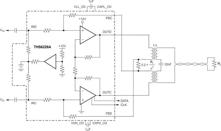
Typical VDSL2 Line Driver Circuit Using One Port of the THS6226A

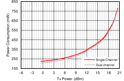
Power Consumption vs Tx
