SLOS932 December 2015 THS7530-Q1
PRODUCTION DATA.
- 1 Features
- 2 Applications
- 3 Description
- 4 Revision History
- 5 Pin Configuration and Functions
- 6 Specifications
- 7 Parameter Measurement Information
- 8 Detailed Description
- 9 Application and Implementation
- 10Power Supply Recommendations
- 11Layout
- 12Device and Documentation Support
- 13Mechanical, Packaging, and Orderable Information
パッケージ・オプション
メカニカル・データ(パッケージ|ピン)
- PWP|14
サーマルパッド・メカニカル・データ
- PWP|14
発注情報
8 Detailed Description
8.1 Overview
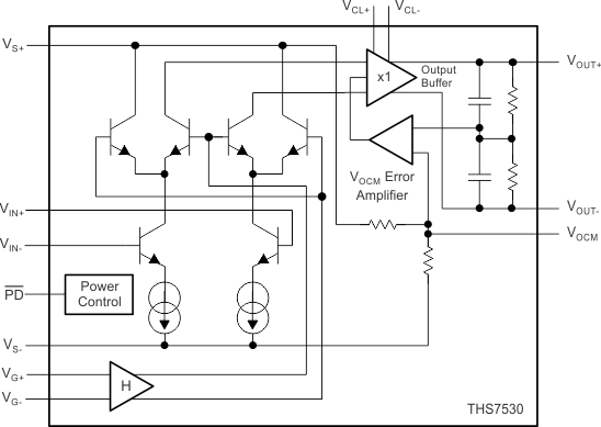
The THS7530-Q1 device is a fully-differential amplifier with 300-MHz bandwidth and with continually-variable gain from 11.6 dB to 46.5 dB. This amplifier together with an automatic gain control (AGC) circuit will precisely established a desired amplitude at its output.
The input architecture is a modified Gilbert cell. The output from the Gilbert cell is converted to a voltage and buffered to the output as a fully-differential signal. A summing node between the outputs is used to compare the output common-mode voltage to the VOCM input. The VOCM error amplifier then servos the output common-mode voltage to maintain it equal to the VOCM input. Left unterminated, VOCM is set to midsupply by internal resistors.
The gain control input is conditioned to give linear-in-dB gain control (block H). The gain control input is a differential signal from 0 V to 0.9 V which varies the gain from 11.6 dB to 46.5 dB.
VCL+ and VCL– provide inputs that limit the output voltage swing of the amplifier.
8.2 Functional Block Diagram

8.3 Feature Description
The main features of the THS7530-Q1 device are continually-variable gain control, common-mode voltage control, output voltage clamps, and power-down mode.
8.3.1 Continually-Variable Gain Control
The amplifier gain in dB is a linear function of the gain control voltage, which has a range of 0 V to 0.9 V. The slope of the gain control input is 38.8 dB/V with a gain range of 11.6 dB to 46.5 dB, which is 3.8 to 211.3 V/V, respectively. The bandwidth of the gain control is 15 MHz, typically.
The gain control is a differential input to reduce noise due to ground bounce, coupling, and so forth. The negative gain-control input VG– can be below the negative supply by as much as 600 mV.
8.3.2 Common-Mode Voltage Control
The common-mode voltage control sets the common-mode voltage of the differential output. The gain of the control voltage is 1 V/V with a range of 1.75 V to 3.25 V above the negative supply. If unconnected, the common-mode voltage control is at mid-supply, typically 2.5 V above the negative supply. The bandwidth of the common-mode voltage control is an impressive 32 MHz.
8.3.3 Output Voltage Clamps
Separate inputs, VCL– and VCL+, establish the minimum and maximum output voltages, respectively. The typical error of the output voltage compared to the clamp voltage is only 25 mV. This feature can be used to avoid saturating the inputs of a receiving device, thereby precluding long recovery times in the signal path.
8.3.4 Power-Down Mode
To minimize power consumption when idle, the THS7530-Q1 device has an active-low power-down control that reduces the quiescent current from 40 mA to 350 µA. The turnon delay is only 820 ns.
When in power-down mode, the THS7530-Q1 device has a 80-dB forward isolation to allow other devices to drive the same signal path with minimal interference from the idle THS7530-Q1 device.
8.4 Device Functional Modes
The THS7530-Q1 device has two functional modes: full-power mode and power-down mode. The power-down mode reduces the quiescent current of the device to 350 µA from a typical value of 40 mA.
With a turnon time of only 820 ns and a turnoff time of 500 ns, the power-down mode can be used to greatly reduce the average power consumption of the device without sacrificing system performance.