JAJSJO7E December 2002 – August 2020 THS7530
PRODUCTION DATA
- 1 特長
- 2 アプリケーション
- 3 概要
- 4 Revision History
- 5 Pin Configuration and Functions
- 6 Specifications
- 7 Parameter Measurement Information
- 8 Detailed Description
- 9 Application and Implementation
- 10Power Supply Recommendations
- 11Layout
- 12Device and Documentation Support
- 13Mechanical, Packaging, and Orderable Information
パッケージ・オプション
メカニカル・データ(パッケージ|ピン)
- PWP|14
サーマルパッド・メカニカル・データ
- PWP|14
発注情報
6.7 Typical Characteristics
Measured using the AC test circuit shown in Figure 7-1 (unless otherwise noted).
Table 6-1 Table Of Graphs
| FIGURE | ||
|---|---|---|
| Voltage Gain to Load | vs Frequency (Input at 45 dBm) | Figure 6-1 |
| Gain and Gain Error | vs VG+ | Figure 6-2 |
| Noise Figure | vs Frequency | Figure 6-3 |
| Output Intercept Point | vs Frequency | Figure 6-4 |
| 1-dB Compression Point | vs Frequency | Figure 6-5 |
| Total Input Voltage Noise | vs Frequency | Figure 6-6 |
| Intermodulation Distortion | vs Frequency | Figure 6-7 |
| Harmonic Distortion | vs Frequency | Figure 6-8 |
| S-Parameters | vs Frequency | Figure 9-7 |
| Differential Input Impedance of Main Amplifier | vs Frequency | Figure 9-8 |
| Differential Output Impedance of Main Amplifier | vs Frequency | Figure 6-9 |
| VG+ Input Impedance | vs Frequency | Figure 6-10 |
| VOCM Input Impedance | vs Frequency | Figure 6-11 |
| Common-Mode Rejection Ratio | vs Frequency | Figure 6-12 |
| Step Response: 2 VPP | vs Time | Figure 6-13 |
| Step Response: Rising Edge | vs Time | Figure 6-14 |
| Step Response: Falling Edge | vs Time | Figure 6-15 |
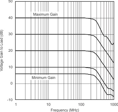
| Gain is taken at load. | Add 6 dB to refer to amplifier output | |
| PIN = –45 dBm | ||
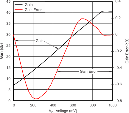 Figure 6-2 Gain and Gain Error vs VG+
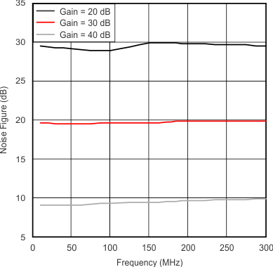
| Terminated input |
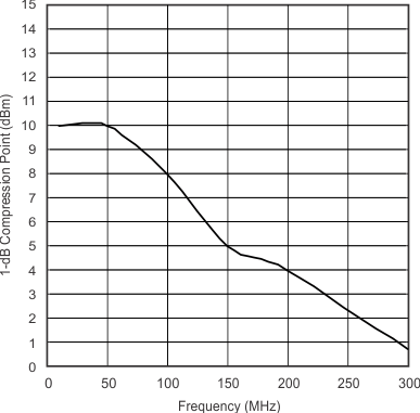
| Taken at load. | Add 3 dB to refer to amplifier output. | |
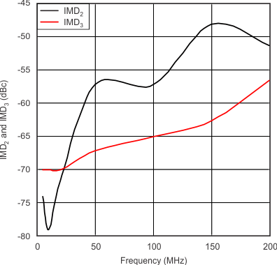
| VG+ = 1 V | VO = 1 VPP (composite) | RL = 400 Ω |
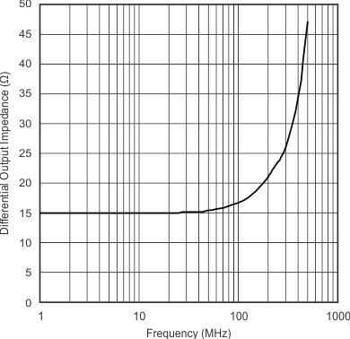 Figure 6-9 Differential Output Impedance of Main Amplifier vs Frequency
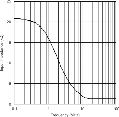 Figure 6-11 VOCM Input Impedance vs Frequency
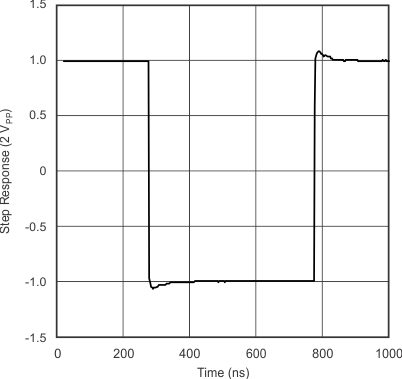
| RL = 400 Ω | At amplifier output and minimum gain | |
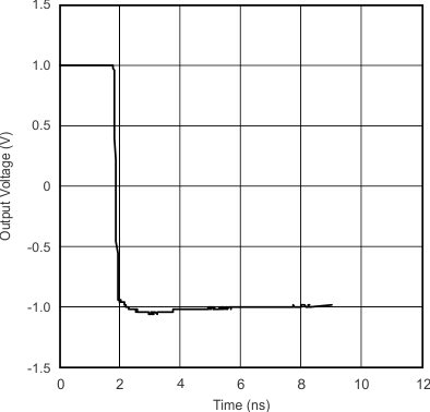
| RL = 400 Ω | At amplifier output and minimum gain | ||
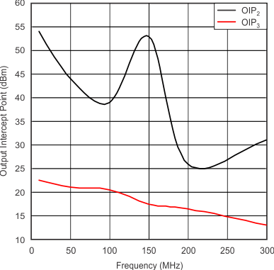
| Taken at load. | Add 3 dB to refer to amplifier output. | |
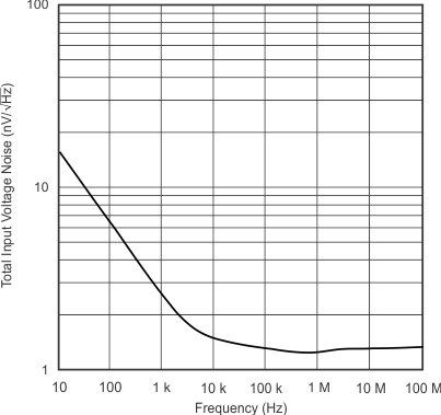 Figure 6-6 Total Input Voltage Noise vs Frequency
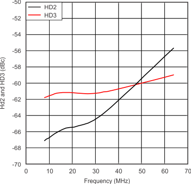
| VG+ = 1 V | VO = 1 VPP | RL = 400 Ω |
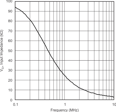 Figure 6-10 VG+ Input Impedance vs Frequency
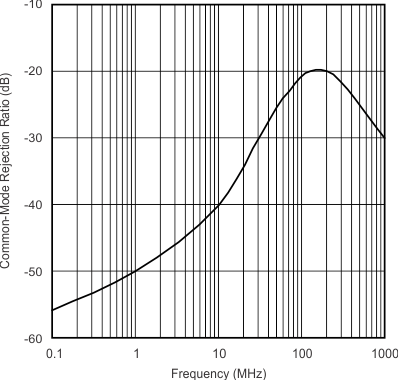 Figure 6-12 Common-Mode Rejection Ratio vs Frequency
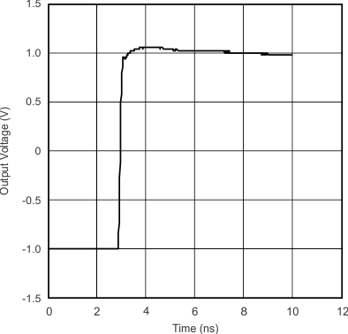
| RL = 400 Ω | At amplifier output and minimum gain | |