JAJSJO7E December 2002 – August 2020 THS7530
PRODUCTION DATA
- 1 特長
- 2 アプリケーション
- 3 概要
- 4 Revision History
- 5 Pin Configuration and Functions
- 6 Specifications
- 7 Parameter Measurement Information
- 8 Detailed Description
- 9 Application and Implementation
- 10Power Supply Recommendations
- 11Layout
- 12Device and Documentation Support
- 13Mechanical, Packaging, and Orderable Information
パッケージ・オプション
メカニカル・データ(パッケージ|ピン)
- PWP|14
サーマルパッド・メカニカル・データ
- PWP|14
発注情報
9.1 Application Information
The THS7530 device is designed to work in a wide variety of applications requiring continuously variable gain and a fully-differential signal path. The common-mode voltage control and the output voltage clamps enable the THS7530 device to drive a diverse array of receiving circuits.
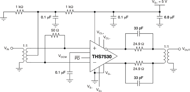 Figure 9-1 EVM Schematic: Designed for Use With Typical 50-Ω RF Test Equipment
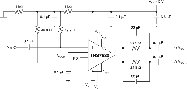 Figure 9-2 AC-Coupled Single-Ended Input With AC-Coupled Differential Output
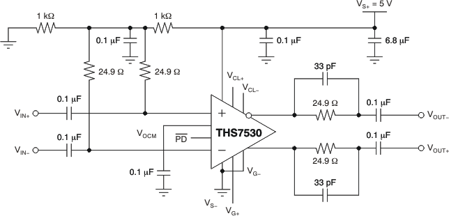 Figure 9-3 AC-Coupled Differential Input With AC-Coupled Differential Output
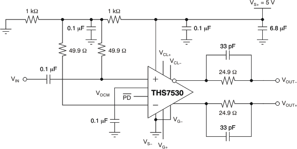 Figure 9-4 DC-Coupled Single-Ended Input With DC-Coupled Differential Output
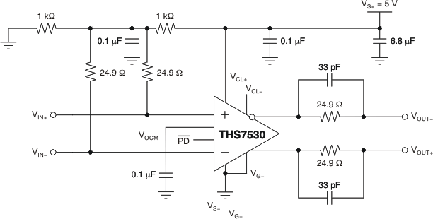 Figure 9-5 DC-Coupled Differential Input With DC-Coupled Differential Output