JAJSDS2A September 2017 – February 2022 TIC10024-Q1
PRODUCTION DATA
- 1 特長
- 2 アプリケーション
- 3 概要
- 4 Revision History
- 5 Pin Configuration and Functions
- 6 Specifications
- 7 Parameter Measurement Information
-
8 Detailed Description
- 8.1 Overview
- 8.2 Functional Block Diagram
- 8.3
Feature Description
- 8.3.1 VS Pin
- 8.3.2 VDD Pin
- 8.3.3 Device Initialization
- 8.3.4 Device Trigger
- 8.3.5 Device Reset
- 8.3.6 VS Under-Voltage (UV) Condition
- 8.3.7 VS Over-Voltage (OV) Condition
- 8.3.8 Switch Inputs Settings
- 8.3.9 Interrupt Generation and INT Assertion
- 8.3.10 Temperature Monitor
- 8.3.11 Parity Check And Parity Generation
- 8.3.12 Cyclic Redundancy Check (CRC)
- 8.4 Device Functional Modes
- 9 Programming
- 10Application and Implementation
- 11Power Supply Recommendations
- 12Layout
- 13Device and Documentation Support
- 14Mechanical, Packaging, and Orderable Information
パッケージ・オプション
メカニカル・データ(パッケージ|ピン)
- DCP|38
サーマルパッド・メカニカル・データ
- DCP|38
発注情報
8.4.2 Polling Mode
The polling mode can be activated to reduce current drawn in ignition-off condition to conserve battery charge. Unlike the continuous mode, the current sources/sinks do not stay on continuously in the polling mode. Instead, they are turned on/off sequentially from IN0 to IN23 and cycled through each individual input channel. The microcontroller can be put to sleep to reduce overall system power. If a switch status change (SSC) is detected by the TIC10024-Q1, the INT pin (if enabled for the input channel) is asserted low (and the SSC bit in INT_STAT register and the SPI status flag SSC are also asserted to logic 1). The INT pin assertion can be used to wake up the system regulator which, in turn, wakes up the microcontroller as described in section Microcontroller Wake-Up. The microcontroller can then use SPI communication to read the switch status information.
The polling is activated when the TRIGGER bit in the CONFIG register is set to logic 1.
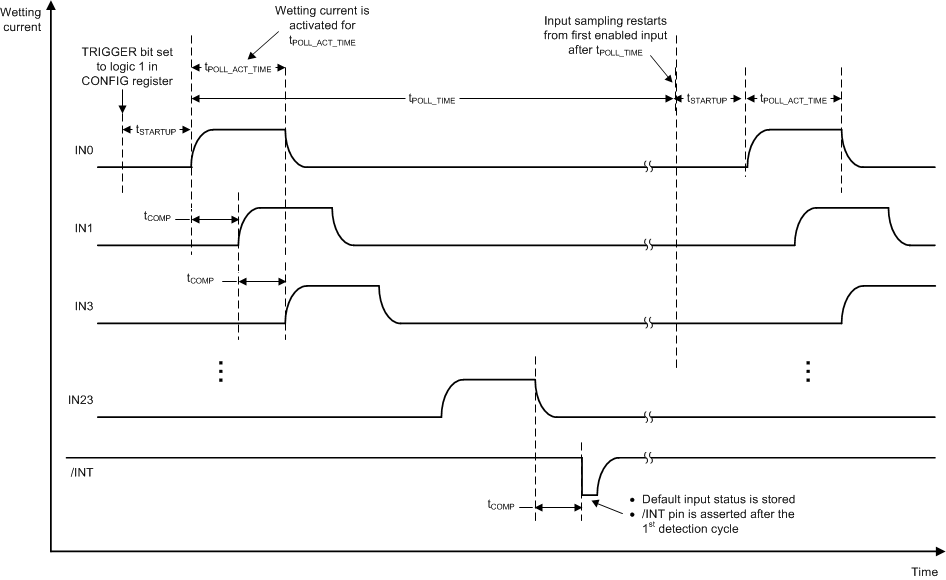
In polling mode, wetting current is applied to each input for a pre-programmed polling active time between 64 μs and 2048 μs, set by the POLL_ACT_TIME bits in the CONFIG register . At the end of the wetting current application, the input voltage is sampled by the comparator. Each input is cycled through in sequential order from IN0 to IN23. Sampling is repeated at a frequency from 2 ms to 4096 ms, set by the POLL_TIME bits in the CONFIG register . Wetting currents are applied to closed switches only during the polling active time; hence the overall system current consumption can be greatly reduced.
Similar to continuous mode, after the first polling cycle, the switch status of each input (below or above detection threshold) is stored in the register (IN_STAT_COMP) to be used as the default state for subsequent polling cycles. The INT pin is asserted low to notify the microcontroller that the default switch status is ready to be read. The SSC bit in INT_STAT register and the SPI status flag SSC are also asserted to logic 1. The INT_STAT register is cleared and INT pin de-asserted if a SPI READ command is issued to the register. Note the interrupt is always generated after the 1st polling cycle (after the TRIGGER bit in register CONFIG is set to logic 1). In subsequent polling cycles the interrupt is generated only if switch status change is detected.
An example of the timing diagram of the polling mode operation is shown in Figure 8-12.
 Figure 8-12 An Example Of The Polling Sequence In Standard Polling Mode
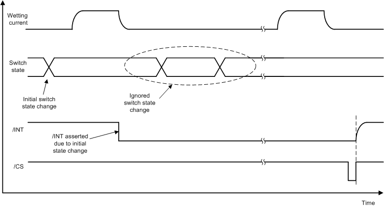
If the switch position changes between two active polling times, no interrupt will be generated and the status register (IN_STAT_COMP) will not reflect such a change. An example is shown in Figure 8-13.
 Figure 8-13 Example For Ignored Switch Position Change Between 2 Wetting Current Cycles