SLLSEN8C September 2015 – June 2017 TL16C752D
PRODUCTION DATA.
- 1 Features
- 2 Applications
- 3 Description
- 4 Revision History
- 5 Description (continued)
- 6 Pin Configurations and Function
- 7 Specifications
-
8 Detailed Description
- 8.1 Overview
- 8.2 Functional Block Diagrams
- 8.3
Feature Description
- 8.3.1
Functional Description
- 8.3.1.1 Trigger Levels
- 8.3.1.2 Hardware Flow Control
- 8.3.1.3 Auto-RTS
- 8.3.1.4 Auto-CTS
- 8.3.1.5 Software Flow Control
- 8.3.1.6 Software Flow Control Example
- 8.3.1.7 Reset
- 8.3.1.8 Interrupts
- 8.3.1.9 Interrupt Mode Operation
- 8.3.1.10 Polled Mode Operation
- 8.3.1.11 Break and Timeout Conditions
- 8.3.1.12 Programmable Baud Rate Generator
- 8.3.1
Functional Description
- 8.4 Device Functional Modes
- 8.5
Register Maps
- 8.5.1 Principals of Operation
- 8.5.2 Receiver Holding Register (RHR)
- 8.5.3 Transmit Holding Register (THR)
- 8.5.4 FIFO Control Register (FCR)
- 8.5.5 Line Control Register (LCR)
- 8.5.6 Line Status Register (LSR)
- 8.5.7 Modem Control Register (MCR)
- 8.5.8 Modem Status Register (MSR)
- 8.5.9 Interrupt Enable Register (IER)
- 8.5.10 Interrupt Identification Register (IIR)
- 8.5.11 Enhanced Feature Register (EFR)
- 8.5.12 Divisor Latches (DLL, DLH)
- 8.5.13 Transmission Control Register (TCR)
- 8.5.14 Trigger Level Register (TLR)
- 8.5.15 FIFO Ready Register
- 8.5.16 Alternate Function Register (AFR)
- 8.5.17 RS-485 Mode
- 8.5.18 IrDA Overview
- 8.5.19 IrDA Encoder Function
- 9 Application and Implementation
- 10Power Supply Recommendations
- 11Layout
- 12Device and Documentation Support
- 13Mechanical, Packaging, and Orderable Information
9 Application and Implementation
NOTE
Information in the following applications sections is not part of the TI component specification, and TI does not warrant its accuracy or completeness. TI’s customers are responsible for determining suitability of components for their purposes. Customers should validate and test their design implementation to confirm system functionality.
9.1 Application Information
The typical implementation is to use the TL16C752D as a dual RS-232 interface, which is intended to operate with a 5-V microprocessor.
9.2 Typical Application
 Figure 39. Typical Application Dual RS-232 Interface
9.2.1 Design Requirements
Include the recommended operating conditions for 3.3 V provided by the controller board, but with the input clock equal to 1.8432 MHz, and include the operating free-air temperature conditions. The controller must have two 8-bit ports, one for the control signals and another for the I/O data. A third port is optional in order to monitor the interruptions and TX/RX ready signals (if it is needed).
9.2.2 Detailed Design Procedure
- Implement the schematic as is shown in Figure 39
- Implement on the controller the READ and WRITE routines in order to meet the timing requirements of the Timing Requirements, use Figure 1 and Figure 2 as a guideline.
- Initialize all the configuration registers. TI recommends not to obviate the default settings and initialize all of the set of configuration registers. The base set of registers that are used during high-speed data transfer have a straightforward access method. The extended function registers require special access bits to be decoded along with the address lines. The following guide helps with programming these registers. Note that the descriptions are for individual register access. Some streamlining through interleaving can be obtained when programming all the registers.
- Set baud rate to VALUE1, VALUE2 Read LCR (03), save in temp Set LCR (03) to 80 Set DLL (00) to VALUE1 Set DLM (01) to VALUE2 Set LCR (03) to temp
- Set Xoff1, Xon1 to VALUE1, VALUE2 Read LCR (03), save in temp Set LCR (03) to BF Set Xoff1 (06) to VALUE1 Set Xon1 (04) to VALUE2 Set LCR (03) to temp
- Set Xoff2, Xon2 to VALUE1, VALUE2 Read LCR (03), save in temp Set LCR (03) to BF Set Xoff2 (07) to VALUE1 Set Xon2 (05) to VALUE2 Set LCR (03) to temp
- Set software flow control mode to VALUE Read LCR (03), save in temp Set LCR (03) to BF Set EFR (02) to VALUE Set LCR (03) to temp
- Set flow control threshold to VALUE Read LCR (03), save in temp1 Set LCR (03) to BF Read EFR (02), save in temp2 Set EFR (02) to 10 + temp2 Set LCR (03) to 00 Read MCR (04), save in temp3 Set MCR (04) to 40 + temp3 Set TCR (06) to VALUE Set LCR (03) to BF Set EFR (02) to temp2 Set LCR (03) to temp1 Set MCR (04) to temp3
- Set xmt and rcv FIFO thresholds to VALUE Read LCR (03), save in temp1 Set LCR (03) to BF Read EFR (02), save in temp2 Set EFR (02) to 10 + temp2 Set LCR (03) to 00 Read MCR (04), save in temp3 Set MCR (04) to 40 + temp3 Set TLR (07) to VALUE Set LCR (03) to BF Set EFR (02) to temp2 Set LCR (03) to temp1 Set MCR (04) to temp3
- Read FIFORdy register Read MCR (04), save in temp1 Set temp2 = temp1 × EF Set MCR (04), save in temp2 Read FRR (07), save in temp2 Pass temp2 back to host Set MCR (04) to temp1
The designer can use Figure 39 as a guideline to configure each channel of the UART.
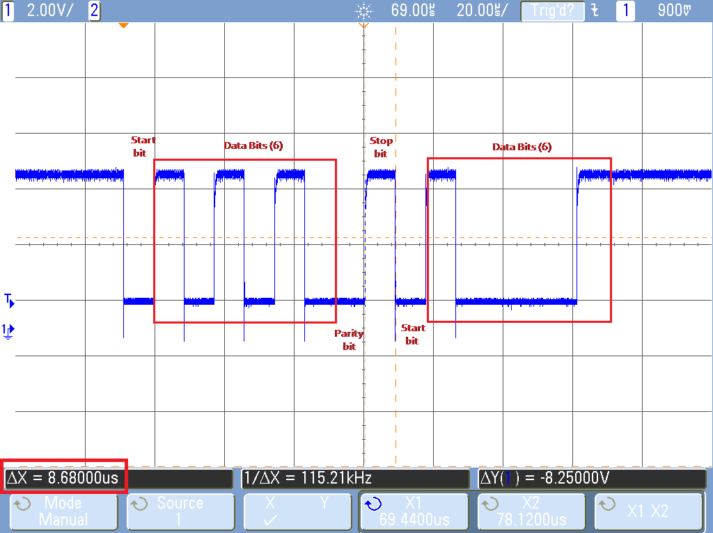
9.2.3 Application Curves


